28F008C3 Ver la hoja de datos (PDF) - Intel
Número de pieza
componentes Descripción
Fabricante
28F008C3 Datasheet PDF : 59 Pages
| |||
3 VOLT ADVANCED+ BOOT BLOCK
E
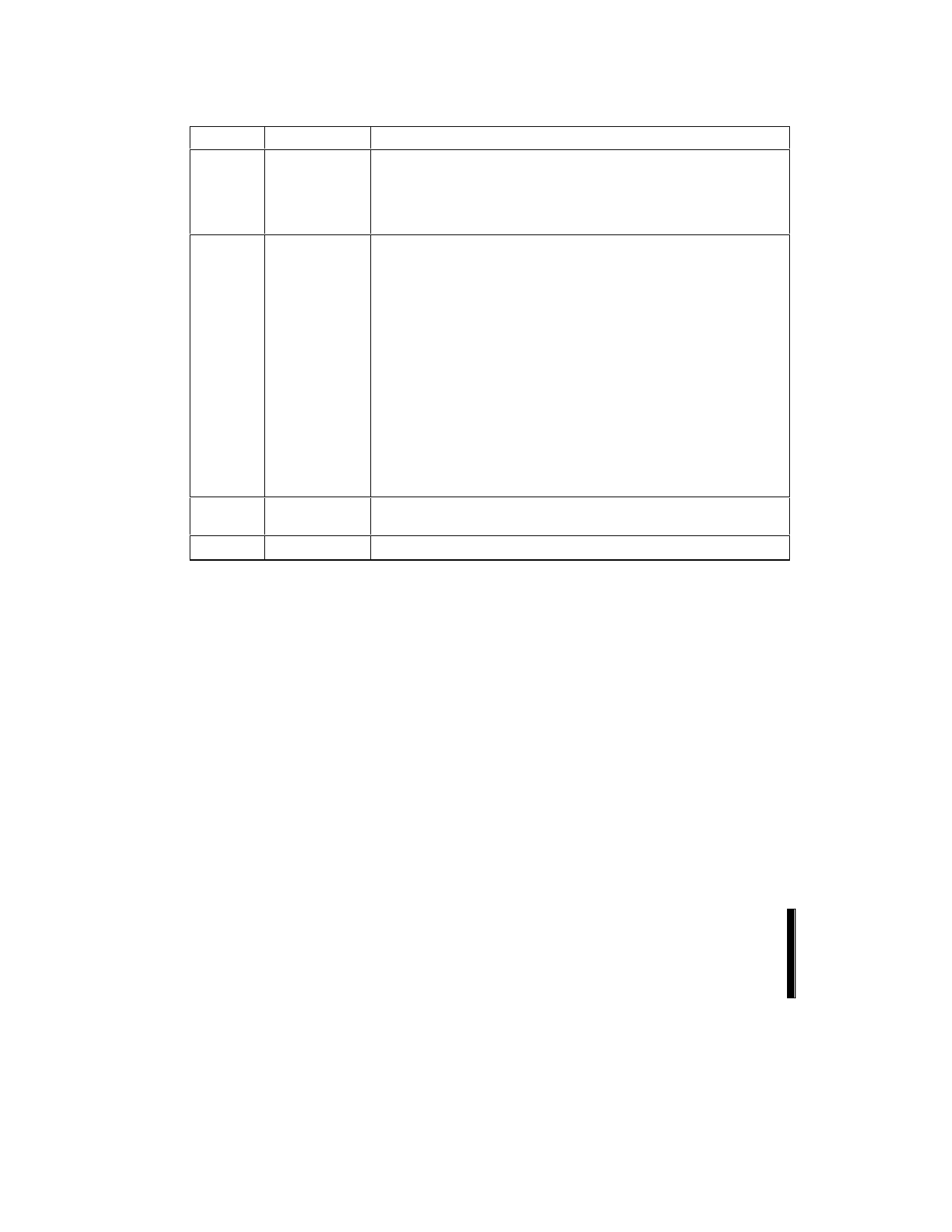
Symbol
VCCQ
VPP
GND
NC
Table 2. 3 Volt Advanced+ Boot Block Pin Descriptions (Continued)
Type
Name and Function
INPUT
I/O POWER SUPPLY: Supplies power for input/output buffers.
[2.7 V–3.6 V] This input should be tied directly to VCC.
[1.65 V– 2.5 V] Lower I/O power supply voltage available upon request.
Contact your Intel representative for more information.
INPUT/
SUPPLY
PROGRAM/ERASE POWER SUPPLY: [1.65 V–3.6 V or 11.4 V–12.6 V]
Operates as a input at logic levels to control complete device protection.
Supplies power for accelerated program and erase operations in 12 V ±
5% range. This pin cannot be left floating.
Lower VPP ≤ VPPLK, to protect all contents against Program and
Erase commands.
Set VPP = VCC for in-system read, program and erase operations. In
this configuration, VPP can drop as low as 1.65 V to allow for resistor or
diode drop from the system supply. Note that if VPP is driven by a logic
signal, VIH = 1.65. That is, VPP must remain above 1.65V to perform in-
system flash modifications.
Raise VPP to 12 V ± 5% for faster program and erase in a production
environment. Applying 12 V ± 5% to VPP can only be done for a
maximum of 1000 cycles on the main blocks and 2500 cycles on the
parameter blocks. VPP may be connected to 12 V for a total of 80 hours
maximum. See Section 3.4 for details on VPP voltage configurations.
SUPPLY
GROUND: For all internal circuitry. All ground inputs must be
connected.
NO CONNECT: Pin may be driven or left floating.
2.2 Block Organization
The 3 Volt Advanced+ Boot Block is an
asymmetrically-blocked architecture that enables
system integration of code and data within a single
flash device. Each block can be erased
independently of the others up to 100,000 times.
For the address locations of each block, see the
memory maps in Appendix E and F.
2.2.1
PARAMETER BLOCKS
The 3 Volt Advanced+ Boot Block flash memory
architecture includes parameter blocks to facilitate
storage of frequently updated small parameters
(i.e., data that would normally be stored in an
EEPROM). Each device contains eight parameter
blocks of 8-Kbytes/4-Kwords (8,192 bytes/4,096
words).
2.2.2
MAIN BLOCKS
After the parameter blocks, the remainder of the
array is divided into equal size (64-Kword/32-
Kword; 65,536 bytes/32,768 words) main blocks for
data or code storage. Each 8-Mbit, 16-Mbit, or
32-Mbit device contains 15, 31, or 63 main blocks,
respectively.
10
PRODUCT PREVIEW
Share Link: 