FM207-H Ver la hoja de datos (PDF) - Shenzhen Luguang Electronic Technology Co., Ltd
Número de pieza
componentes Descripción
Fabricante
FM207-H
Shenzhen Luguang Electronic Technology Co., Ltd

FM207-H Datasheet PDF : 7 Pages
| |||
Chip Silicon Rectifier
FM201 THRU FM207
Formosa MS
2.0A Surface Mount General Purpose
Rectifiers - 50V-1000V
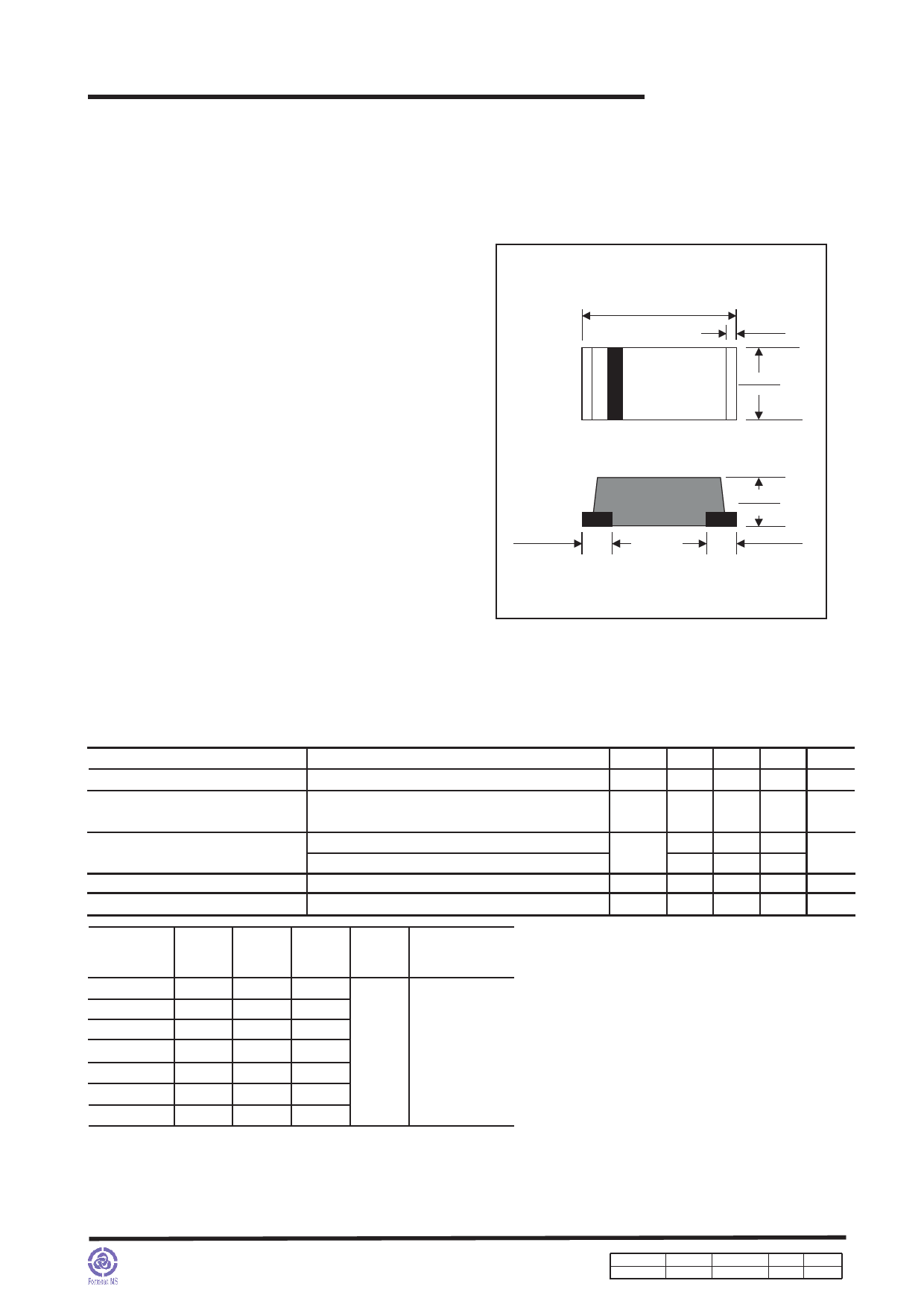
Package outline
Features
• Batch process design, excellent power dissipation offers
better reverse leakage current and thermal resistance.
• Low profile surface mounted application in order to
optimize board space.
• High current capability.
• High surge capability.
• Glass passivated chip junction.
• Lead-free parts meet environmental standards of
MIL-STD-19500 /228
• Suffix "-H" indicates Halogen-free parts, ex. FM201-H.
Mechanical data
• Epoxy:UL94-V0 rated flame retardant
• Case : Molded plastic, DO-214AC / SMA
• Terminals : Solder plated, solderable per
MIL-STD-750, Method 2026
• Polarity : Indicated by cathode band
• Mounting Position : Any
• Weight : Approximated 0.05 gram
SMA
0.196(4.9)
0.180(4.5)
0.012(0.3) Typ.
0.106(2.7)
0.091(2.3)
0.032(0.8) Typ.
0.068(1.7)
0.060(1.5)
0.032 (0.8) Typ.
Dimensions in inches and (millimeters)
Maximum ratings and Electrical Characteristics (AT TA=25oC unless otherwise noted)
PARAMETER
CONDITIONS
Symbol MIN. TYP. MAX. UNIT
Forward rectified current
See Fig.2
IO
2.0
A
Forward surge current
Reverse current
Diode junction capacitance
Storage temperature
8.3ms single half sine-wave superimposed on
rate load (JEDEC methode)
VR = VRRM TJ = 25OC
VR = VRRM TJ = 125OC
f=1MHz and applied 4V DC reverse voltage
IFSM
50
A
5.0
IR
μA
125
CJ
30
pF
TSTG
-65
+175 OC
SYMBOLS
FM201
FM202
FM203
FM204
FM205
FM206
FM207
*1
VRRM
(V)
50
100
200
400
600
800
1000
V
*
RMS
2
(V)
35
70
140
280
420
560
700
*3
VR
(V)
50
100
200
400
600
800
1000
*4
VF
(V)
1.10
Operating
temperature
TJ, (OC)
-55 to +150
*1 Repetitive peak reverse voltage
*2 RMS voltage
*3 Continuous reverse voltage
*4 Maximum forward voltage@IF=2.0A
http://www.formosams.com/
TEL:886-2-22696661
FAX:886-2-22696141
Page 2
Document ID Issued Date
DS-121107 2008/02/10
Revised Date Revision
2010/03/09
D
Page.
7
Share Link: