EDI88130CP100CM Ver la hoja de datos (PDF) - White Electronic Designs Corporation
Número de pieza
componentes Descripción
Fabricante
EDI88130CP100CM Datasheet PDF : 8 Pages
| |||
White Electronic Designs
EDI88128C
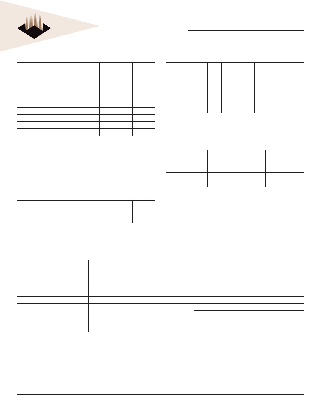
ABSOLUTE MAXIMUM RATINGS
Parameter
Unit
Voltage on any pin relative to VSS
-0.5 to 7.0
V
Operating Temperature TA (Ambient)
Commercial
0 to +70
°C
Industrial
-40 to +85
°C
Military
-55 to +125
°C
Storage Temperature, Plastic
-65 to +150
°C
Power Dissipation
1
W
Output Current
20
mA
Junction Temperature, TJ
175
°C
NOTE:
Stress greater than those listed under "Absolute Maximum Ratings" may cause
permanent damage to the device. This is a stress rating only and functional operation
of the device at these or any other conditions greater than those indicated in the
operational sections of this specification is not implied. Exposure to absolute maximum
rating conditions for extended periods may affect reliability.
CAPACITANCE
TA = +25°C
Parameter
Symbol
Address Lines
CI
Input/Output Lines CO
Condition
VIN = VCC or VSS, f = 1.0MHz
VOUT = VCC or VSS, f = 1.0MHz
Max Unit
12 pF
14 pF
These parameters are sampled, not 100% tested.
TRUTH TABLE
OE# CS1# CS2# WE#
Mode
XHXX
Standby
XXLX
Standby
X X L X Output Deselect
H L H H Output Deselect
L LHH
Read
XLHL
Write
Output
High Z
High Z
High Z
High Z
Data Out
Data In
Power
Icc2, Icc3
Icc2, Icc3
Icc1
Icc1
Icc1
Icc1
Recommended Operating Conditions
Parameter
Symbol Min
Supply Voltage
VCC
4.5
Supply Voltage
VSS
0
Input High Voltage
VIH
2.2
Input Low Voltage
VIL
-0.3
Typ Max Unit
5.0
5.5
V
0
0
V
— VCC +0.5 V
—
+0.8
V
DC CHARACTERISTICS
VCC = 5V, -55°C ≤ TA ≤ +125°C
Parameter
Symbol Conditions
Min
Typ
Max
Units
Input Leakage Current
ILI VIN = 0V to VCC
-5
—
+5
µA
Output Leakage Current
ILO VI/O = 0V to VCC, CS1# ≥ VIH and/or CS2# ≤ VIL
-10
—
+10
µA
Operating Power Supply Current
ICC1 WE#, CS1# = VIL, II/O = 0mA, Min Cycle
CS2# = VIH
(70-85ns) —
(100ns)
—
120
mA
110
mA
Standby (TTL) Power Supply Current ICC2 CS1# ≥ VIH and/or CS2# ≤ VIL, VIN ≥ VIH or ≤ VIL
—
10
mA
CS1# ≥ VCC -0.2V and/or CS2# ≤ VCC+0.2V
C
—
1
5
mA
Full Standby Power Supply Current
ICC3 VIN ≥ VCC -0.2V or VIN ≤ 0.2V
LP
—
—
1
mA
Output Low Voltage
VOL IOL = 2.1mA
—
—
0.4
V
Output High Voltage
VOH IOH = -1.0mA
2.4
—
—
V
NOTE: DC test conditions : VIL = 0.3V, VIH = VCC -0.3V
White Electronic Designs Corp. reserves the right to change products or specifications without notice.
April 2005
Rev. 17
2
White Electronic Designs Corporation • (602) 437-1520 • www.wedc.com
Share Link: 