DTC123JCA Ver la hoja de datos (PDF) - Willas Electronic Corp.
Número de pieza
componentes Descripción
Fabricante
DTC123JCA Datasheet PDF : 2 Pages
| |||

WILLAS
FM120-M+
DTC123JCA THRU
1.0NA SPUNRFDACiEgMitOaUlNTT rSaCnHOsTiTsKtYoBrARRIER RECTIFIERS -20V- 200V
FM1200-M+
SOD-123+ PACKAGE
Typical CharacterPiasctkicagse outline
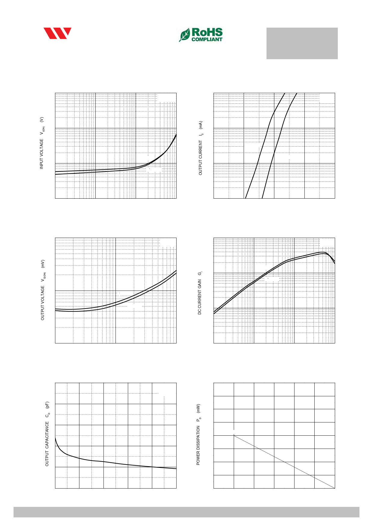
Features ON Characteristics
OFF Characteristics
100 • Batch process design, excellent power dissipation offers
10
better reverse leakage current and thermaVlOr=e0.s3Vistance.
SOD-123H
• Low profile surface mounted application in order to
30 optimize board space.
3
• Low power loss, high efficiency.
• High current capability, low forward voltage drop.
10 • High surge capability.
1
0.146(3.7)
0.130(3.3)
• Guardring for overvoltage protection.
3 • Ultra high-speed switching.
0.3
• Silicon epitaxial planar chip, metal silicon junction.
• Lead-free parts meet environmenTat=a2l5℃standards of
1 MIL-STD-19500 /228
0.1
• RoHS product for packing code suffix "GT"a=100℃
Halogen free product for packing code suffix "H"
0.3 Mechanical data
0.03
Ta=100℃
Ta=25℃
• Epoxy : UL94-V0 rated flame retardant
0.1
•0.1 Case 0:.3Molded p1 lastic, S3 OD-12310H
30
100
•
Terminals
:
OUTPUT CURRENT
Plated terminals
,IOs
o
(mA)
lder
a
b
l
e
per
,
MIL-STD-750
0.01
0.2
0.4
0.6
0.8
0.031(0.8) Typ.
INPUT VOLTAGE VI(OFF) (V)
Pb Free Produc
VCC=5V
0.012(0.3) Typ.
0.071(1.8)
0.056(1.4)
0.040(1.0)
0.024(0.6)
1.0
0.031(0.8) Typ.
Method 2026
• Polarity : IndicateVd by ca—th—odeI band
O(ON)
O
1000 • Mounting Position : Any
1000
• Weight : Approximated 0.011 gram
IO/II=20
DimenGsion—s in—inchIes and (millimeters)
I
O
VO=5V
300
MAXIMUM RATINGS AND ELECTRICAL CHARACTERISTICS
300
Ratings at 25℃ ambient temperature unless otherwise specified.
100
Single phase half wave, 60Hz, resistive of inductive load.
For capacitive load, derate current by 20%
Ta=100℃
Ta=25℃
100
RATINGS Ta=100℃
30
SYMBOL FM120-MH FM130-MH FM140-MH FM150-MH FM160-MH FM180-MH FM1100-MH FM1150-MH FM1200-MH
Marking Code
12
13
14
15
16
Maximum Recurrent Peak Reverse VoltageTa=25℃
VRRM
20
30 10 40
50
60
18
10
115 120
80
100
150
200
Maxim3u0m RMS Voltage
VRMS
14
21
28
35
42
56
70
105
140
Maximum DC Blocking Voltage
VDC
20
30 3 40
50
60
80
100
150
200
Maximum Average Forward Rectified Current
IO
1.0
10
Peak For1ward Surge Cu3rrent 8.3 ms sin1g0le half sine-wa30ve IFSM 100
superimposed on rated loaOdU(TJPEUDTECCUmRRetEhNoTd) IO (mA)
1
0.1
0.3
1
33 0
10
30
100
OUTPUT CURRENT IO (mA)
Typical Thermal Resistance (Note 2)
RΘJA
40
Typical Junction Capacitance (Note 1)
Operating Temperature RangeCO
——
V
R
Storag1e0 Temperature Range
CHARACTERISTICS
Maximu8m Forward Voltage at 1.0A DC
Maximum Average Reverse Current at @T A=25℃
Rated D6 C Blocking Voltage
@T A=125℃
CJ
TJ
-55 to +125
120
P —— T
D
a
-55 to +150
TSf=T1GMHz
400
- 65 to +175
Ta=25℃
350
SYMBOL FM120-MH FM130-MH FM140-MH FM150-MH FM160-MH FM180-MH FM1100-MH FM1150-MH FM1200-MH
VF
3000.50
0.70
0.85
0.9
0.92
IR
0.5
250
10
NOTES:
1- Measured at 1 MHZ and applied reverse voltage of 4.0 VDC.
4
2- Thermal Resistance From Junction to Ambient
DTC123JCA
200
150
100
2
50
0
0
4
8
12
16
20
2012-06
REVERSE BIAS VOLTAGE VR (V)
2012-0
0
0
25
50
75
100
125
150
AMBIENT TEMPERWATUIRLELTAa S(℃)ELECTRONIC CORP
WILLAS ELECTRONIC CORP.