CXB1451Q Ver la hoja de datos (PDF) - Sony Semiconductor
Número de pieza
componentes Descripción
Fabricante
CXB1451Q Datasheet PDF : 13 Pages
| |||
CXB1451Q
Operation mode
CXB1451Q supports 3 panel mode and 2 clock mode switched by the PANEL (1, 0) and CKMODE pin
according to the Tab. 5 & 6. The supporting clock rate are summarized in Tab. 7. These pins are open High
TTL inputs.
Tab. 5. Panel Mode select
PANEL1
L
L
H
H
PANEL0
L
H
L
H
Supporting panel size & color
VGA (640 × 480) 18bit color
SVGA (800 × 600) 18bit color
XGA (1024 × 768) 18bit color
not supported
Tab. 6. Clock Mode select
CKMODE
Supporting clock mode
L
2 pixel/ShiftClock (2ppc)
H
1 pixel/ShiftClock (1ppc)
Tab. 7. Operation Mode
Panel Mode Clock Mode
VGA
1 pixel/SftClk
2 pixel/SftClk
SVGA
1 pixel/SftClk
2 pixel/SftClk
XGA
1 pixel/SftClk
2 pixel/SftClk
Color
18bit
18bit
18bit
18bit
18bit
18bit
Shift Clock Dot Clock Serial rate
25MHz 25MHz 600Mbps
12.5MHz 25MHz 600Mbps
40MHz 40MHz 960Mbps
20MHz 40MHz 960Mbps
65MHz 65MHz 1560Mbps
32.5MHz 65MHz 1560Mbps
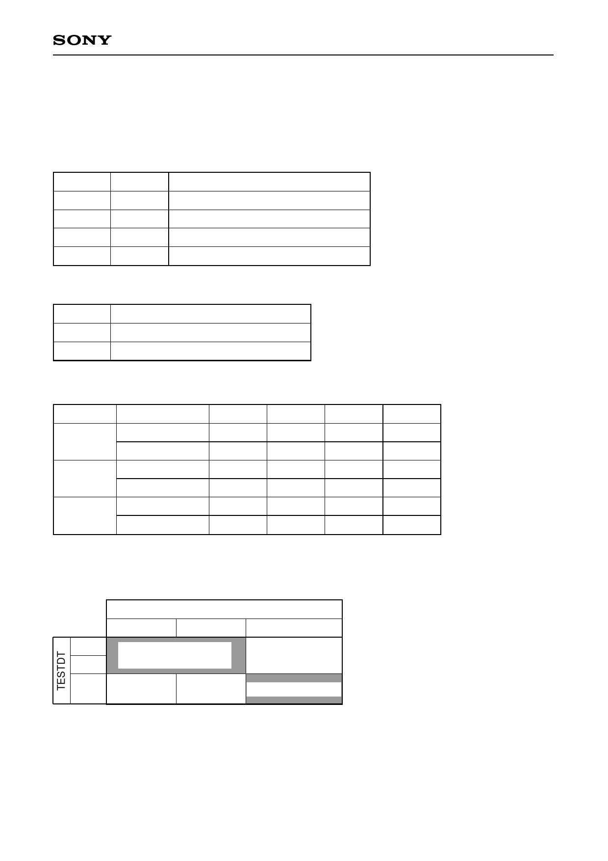
TESTSB/TESTDT pins select the trigger edge of SFTCLK and test mode according to Tab. 8.
Tab. 8. SFTCLK polarity & TEST mode
TESTSB
GND
OPEN
VCC
GND
OPEN
Transmitter operation
trigger = falling edge
Fabricator reserved
TEST mode
VCC
SDATAP = H
SDATAN = L
SDATAP = L
SDATAN = H
Trigger = rising edge
IDLE pin disable differential signal transmission from SDATAP/N pins. It's open High TTL input. Transmission
is disabled when IDLE = High.
–7–
Share Link: 