CS5207-1 Ver la hoja de datos (PDF) - Cherry semiconductor
Número de pieza
componentes Descripción
Fabricante
CS5207-1 Datasheet PDF : 6 Pages
| |||
Applications Information: continued
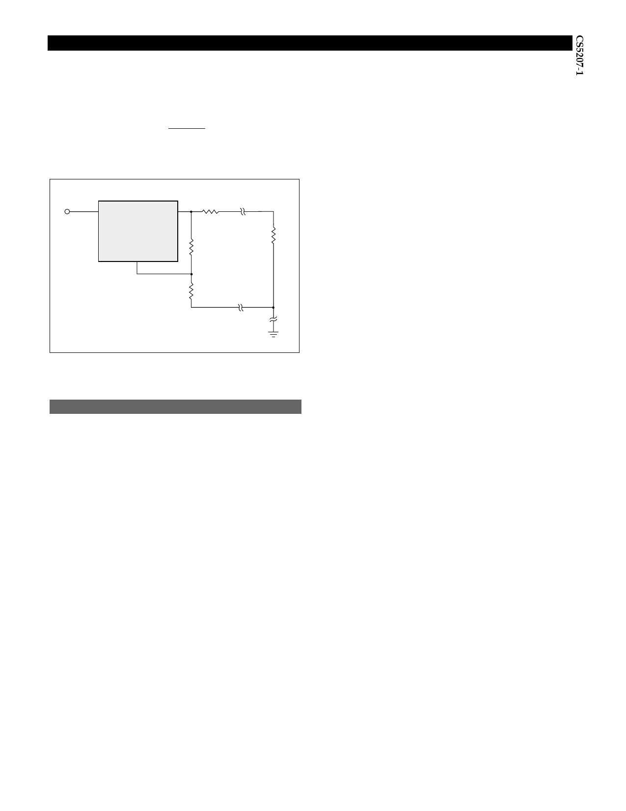
Best load regulation occurs when R1 is connected directly
to the output pin of the regulator as shown in Figure 3. If R1
is connected to the load, RC is multiplied by the divider
ratio and the effective resistance between the regulator and
the load becomes
( ) RC × R1 + R2
R1
RC = conductor parasitic resistance
VIN
VIN
VOUT
conductor parasitic
RC resistance
CS5207-1
R1
Adj
RLOAD
R2
The maximum ambient temperature and the power dissi-
pation are determined by the design while the maximum
junction temperature and the thermal resistance depend
on the manufacturer and the package type.
The maximum power dissipation for a regulator is:
PD(max)={VIN(max)–VOUT(min)}IOUT(max)+VIN(max)IQ
(2)
where
VIN(max) is the maximum input voltage,
VOUT(min) is the minimum output voltage,
IOUT(max) is the maximum output current, for the application
IQ is the maximum quiescent current at IOUT(max).
A heat sink effectively increases the surface area of the
package to improve the flow of heat away from the IC and
into the surrounding air.
Each material in the heat flow path between the IC and the
outside environment has a thermal resistance. Like series
electrical resistances, these resistances are summed to
determine RΘJA, the total thermal resistance between the
junction and the surrounding air.
Figure 3. Grounding scheme for the adjustable output regulator to min-
imize parasitics.
1. Thermal Resistance of the junction to case, RΘJC (°C/W)
2. Thermal Resistance of the case to Heat Sink, RΘCS (°C/W)
3. Thermal Resistance of the Heat Sink to the ambient air,
RΘSA (°C/W)
Calculating Power Dissipation and Heat Sink Requirements
The CS5207-1 linear regulator includes thermal shutdown
and safe operating area circuitry to protect the device.
High power regulators such as this usually operate at high
junction temperatures so it is important to calculate the
power dissipation and junction temperatures accurately to
ensure that an adequate heat sink is used.
The case is connected to VOUT on the CS5207-1, electrical
isolation may be required for some applications. Thermal
compound should always be used with high current regu-
lators such as these.
The thermal characteristics of an IC depend on the follow-
ing four factors:
1. Maximum Ambient Temperature TA (°C)
2. Power dissipation PD (Watts)
3. Maximum junction temperature TJ (°C)
4. Thermal resistance junction to ambient RΘJA (C/W)
These are connected by the equation:
RΘJA = RΘJC + RΘCS + RΘSA
(3)
The value for RΘJA is calculated using equation (3) and the
result can be substituted in equation (1).
The value for RΘJC is normally quoted as a single figure for
a given package type based on an average die size. For a
high current regulator such as the CS5207-1 the majority of
the heat is generated in the power transistor section. The
value for RΘSA depends on the heat sink type, while RΘCS
depends on factors such as package type, heat sink inter-
face (is an insulator and thermal grease used?), and the
contact area between the heat sink and the package. Once
these calculations are complete, the maximum permissible
value of RΘJA can be calculated and the proper heat sink
selected. For further discussion on heat sink selection, see
application note “Thermal Management for Linear
Regulators.”
These four are related by the equation
TJ = TA + PD × RΘJA
(1)
5
Share Link: 