CS5207-1 Ver la hoja de datos (PDF) - Cherry semiconductor
Número de pieza
componentes Descripción
Fabricante
CS5207-1 Datasheet PDF : 6 Pages
| |||
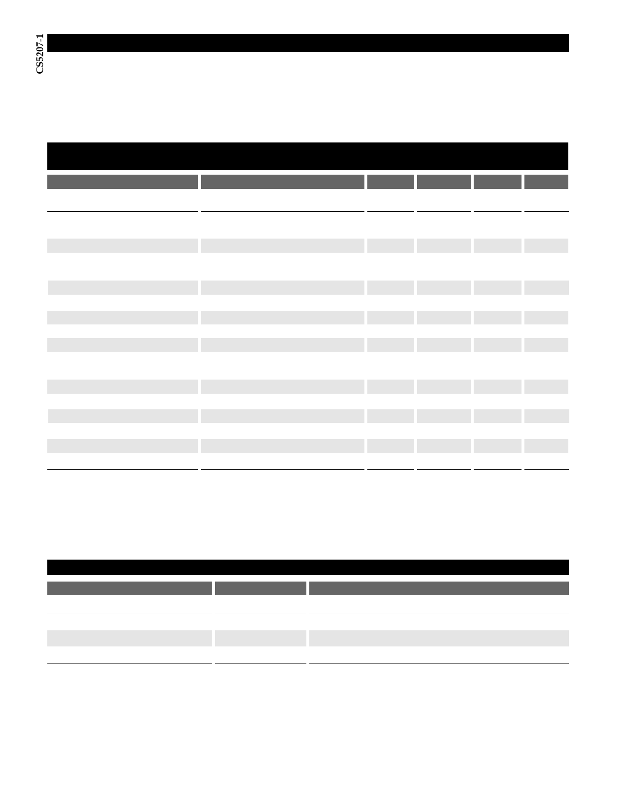
Absolute Maximum Ratings
Supply Voltage, VCC ..................................................................................................................................................................17V
Operating Temperature Range................................................................................................................................-40°C to 70°C
Junction Temperature ............................................................................................................................................................150°C
Storage Temperature Range ..................................................................................................................................-60°C to 150°C
Lead Temperature Soldering
Wave Solder (through hole styles only) .....................................................................................10 sec. max, 260°C peak
Electrical Characteristics: CIN = 10µF, COUT = 22µF Tantalum, VIN – VOUT = 3V, VIN ≤ 15V, 0°C ≤ TA ≤ 70°C, TJ ≤ +150°C,
unless otherwise specified, Ifull load = 7A.
PARAMETER
TEST CONDITIONS
MIN
TYP
MAX
UNIT
s Adjustable Output Voltage
Reference Voltage
(Notes 1 and 2)
Line Regulation
Load Regulation
(Notes 1 and 2)
Dropout Voltage (Note 3)
Current Limit
Minimum Load Current
Adjust Pin Current
Adjust Pin Current Change
Thermal Regulation
Ripple Rejection
Temperature Stability
RMS Output Noise
Thermal Shutdown
Thermal Shutdown Hysteresis
VIN – VOUT = 1.6V; VAdj = 0V
10mA ≤ IOUT ≤ 7A
1.6V ≤ VIN – VOUT ≤ 6V; IOUT = 10mA
VIN – VOUT = 1.6V;
10mA ≤ IOUT ≤ 7A
IOUT = 7A
VIN – VOUT = 3V; TJ ≥ 25°C
VIN – VOUT = 9V
VIN – VOUT = 7V
1.235
(-1.5%)
7.1
1.6V ≤ VIN – VOUT ≤ 4V;
10mA ≤ IOUT ≤ 7A
30ms pulse; TA = 25°C
f = 120Hz; CAdj = 25µF; IOUT = 7A
10Hz ≤ f ≤ 10kHz; TA = 25°C
150
1.254
0.04
0.13
1.4
8.5
1.0
1.2
50
0.2
0.003
80
0.5
0.003
180
25
1.272
V
(+1.5%)
0.20
%
0.5
%
1.55
V
A
A
6
mA
100
µA
5.0
µA
%W
dB
%
%VOUT
°C
°C
Note 1: Load regulation and output voltage are measured at a constant junction temperature by low duty cycle pulse testing. Changes in out-
put voltage due to thermal gradients or temperature changes must be taken into account separately.
Note 2: Specifications apply for an external Kelvin sense connection at a point on the output pin 1/4” from the bottom of the package.
Note 3: Dropout voltage is a measurement of the minimum input/output differential at full load.
PACKAGE PIN #
3L TO-220
1
2
3
Package Pin Description
PIN SYMBOL
FUNCTION
Adj
VOUT
VIN
Adjust pin (low side of the internal reference).
Regulated output voltage (case).
Input voltage.
2
Share Link: 