CS5201-1 Ver la hoja de datos (PDF) - Cherry semiconductor
Número de pieza
componentes Descripción
Fabricante
CS5201-1 Datasheet PDF : 7 Pages
| |||
Applications Information: continued
VIN
C1
VIN
VOUT
CS5201-1
Adj
VREF
R1
IAdj
CAdj
R2
VOUT
C2
Figure 1. Resistor divider scheme.
EXTERNAL SUPPLY
VIN
VOUT
VAdj
VOUT
Short Circuit Protection
The CS5201-1 linear regulator has an absolute maximum
specification of 7V for the voltage difference between VIN
and VOUT. However, the IC may be used to regulate volt-
ages in excess of 7V. The main considerations in such a
design are power-up and short circuit capability.
In most applications, ramp-up of the power supply to VIN
is fairly slow, typically on the order of several tens of mil-
liseconds, while the regulator responds in less than one
microsecond. In this case, the linear regulator begins
charging the load as soon as the VIN to VOUT differential is
large enough that the pass transistor conducts current. The
load at this point is essentially at ground, and the supply
voltage is on the order of several hundred millivolts, with
the result that the pass transistor is in dropout. As the sup-
ply to VIN increases, the pass transistor will remain in
dropout, and current is passed to the load until VOUT
reaches the point at which the IC is in regulation. Further
increase in the supply voltage brings the pass transistor
out of dropout. The result is that the output voltage fol-
lows the power supply ramp-up, staying in dropout until
the regulation point is reached. In this manner, any output
voltage may be regulated. There is no theoretical limit to
the regulated voltage as long as the VIN to VOUT differen-
tial of 7V is not exceeded.
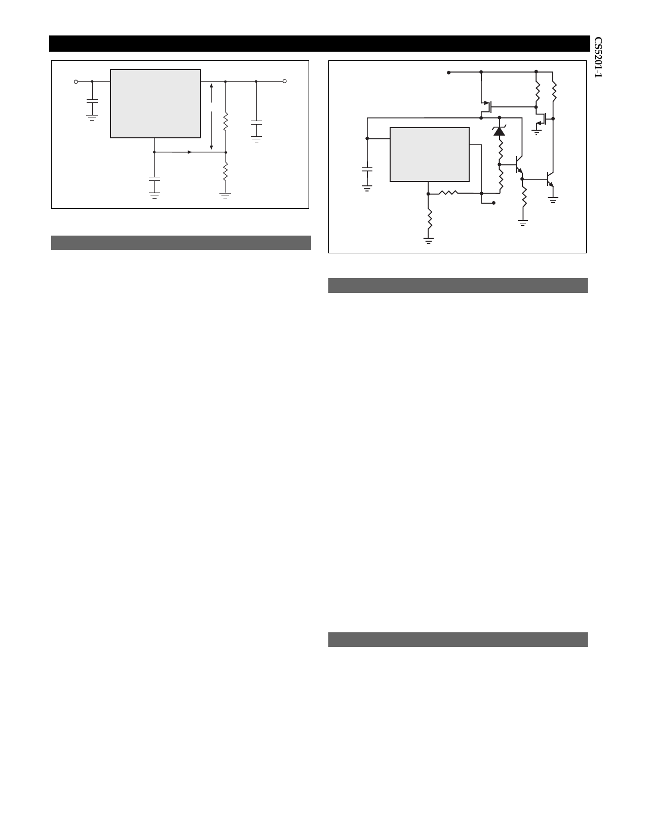
However, the possibility of destroying the IC in a short
circuit condition is very real for this type of design. Short
circuit conditions will result in the immediate operation of
the pass transistor outside of its safe operating area. Over-
voltage stresses will then cause destruction of the pass
transistor before overcurrent or thermal shutdown circuit-
ry can become active. Additional circuitry may be required
to clamp the VIN to VOUT differential to less than 7V if fail-
safe operation is required. One possible clamp circuit is
illustrated in figure 2; however, the design of clamp cir-
cuitry must be done on an application by application basis.
Care must be taken to ensure the clamp actually protects
the design. Components used in the clamp design must be
able to withstand the short circuit condition indefinitely
while protecting the IC.
Figure 2. Short Circuit Protection Circuit for High Voltage Application.
Stability Considerations
The output or compensation capacitor helps determine
three main characteristics of a linear regulator: start-up
delay, load transient response and loop stability.
The capacitor value and type is based on cost, availability,
size and temperature constraints. A tantalum or aluminum
electrolytic capacitor is best, since a film or ceramic capaci-
tor with almost zero ESR can cause instability. The alu-
minum electrolytic capacitor is the least expensive solu-
tion. However, when the circuit operates at low tempera-
tures, both the value and ESR of the capacitor will vary
considerably. The capacitor manufacturersÕ data sheet pro-
vides this information.
A 22µF tantalum capacitor will work for most applications,
but with high current regulators such as the CS5201 the
transient response and stability improve with higher val-
ues of capacitance. The majority of applications for this
regulator involve large changes in load current so the out-
put capacitor must supply the instantaneous load current.
The ESR of the output capacitor causes an immediate drop
in output voltage given by:
ÆV = ÆI ´ ESR
For microprocessor applications it is customary to use an
output capacitor network consisting of several tantalum and
ceramic capacitors in parallel. This reduces the overall ESR
and reduces the instantaneous output voltage drop under
load transient conditions. The output capacitor network
should be as close as possible to the load for the best results.
Protection Diodes
When large external capacitors are used with a linear regu-
lator it is sometimes necessary to add protection diodes. If
the input voltage of the regulator gets shorted, the output
capacitor will discharge into the output of the regulator.
The discharge current depends on the value of the capaci-
tor, the output voltage and the rate at which VIN drops. In
the CS5201-1 linear regulator, the discharge path is
through a large junction and protection diodes are not usu-
ally needed. If the regulator is used with large values of
output capacitance and the input voltage is instantaneous-
ly shorted to ground, damage can occur. In this case, a
diode connected as shown in Figure 3 is recommended.
5
Share Link: 