AS8218 Ver la hoja de datos (PDF) - austriamicrosystems AG
Número de pieza
componentes Descripción
Fabricante
AS8218 Datasheet PDF : 123 Pages
| |||
Data Sheet AS8218 / AS8228
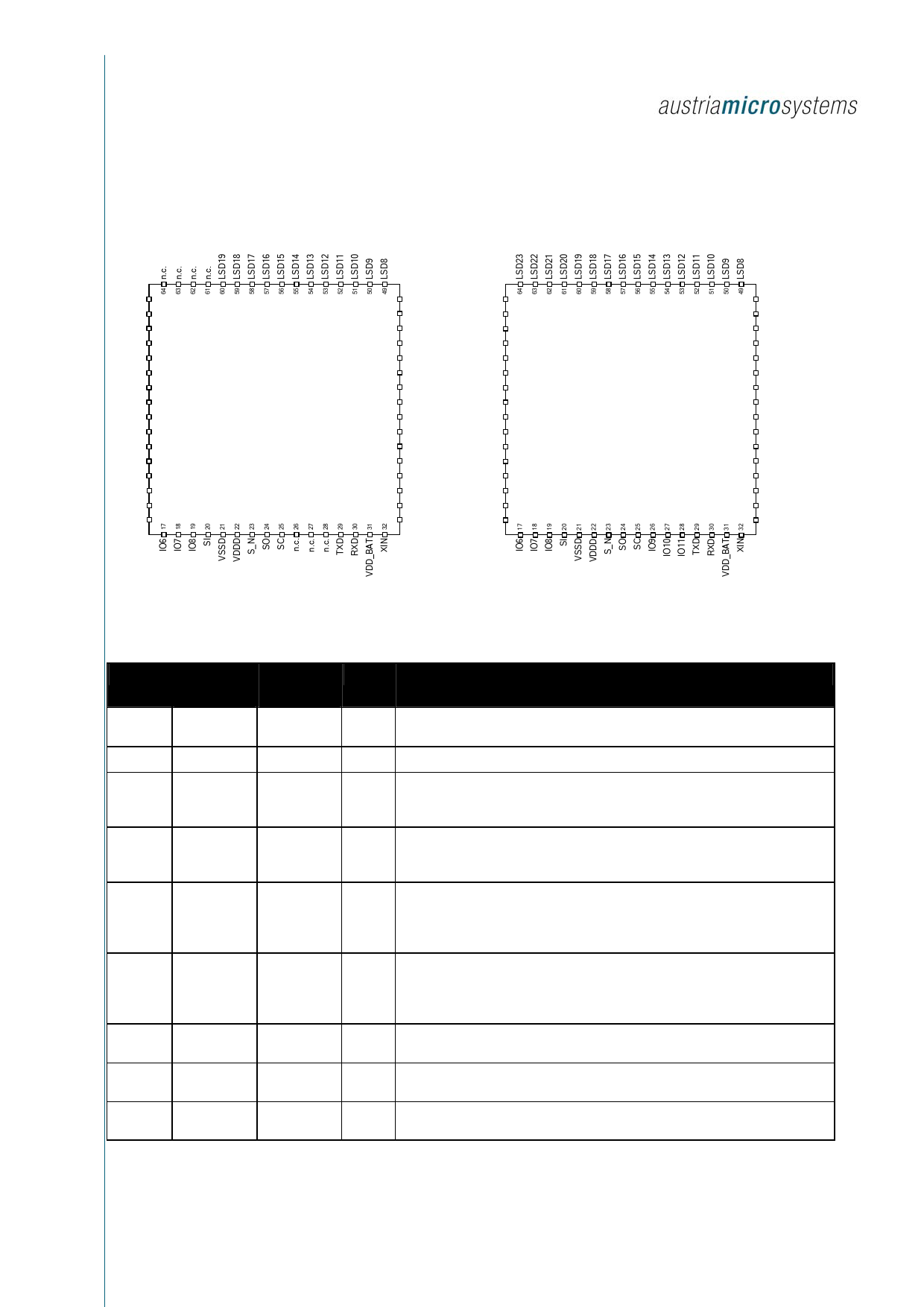
4. Pin Out
VP 1
VN 2
I1P 3
I1N 4
I2P 5
I2N 6
VDDA 7
VSSA 8
IO0 9
IO1 10
IO2 11
IO3 12
VDDD 13
VSSD 14
IO4 15
IO5 16
AS8218
LQFP64
48 LSD7
47 LSD6
46 LSD5
45 LSD4
44 LSD3
43 LSD2
42 LSD1
41 LSD0
40 LBP3
39 LBP2
38 LBP1
37 LBP0
36 n.c.
35 n.c.
34 RES_N
33 XOUT
VP 1
VN 2
I1P 3
I1N 4
I2P 5
I2N 6
VDDA 7
VSSA 8
IO0 9
IO1 10
IO2 11
IO3 12
VDDD 13
VSSD 14
IO4 15
IO5 16
AS8228
LQFP64
48 LSD7
47 LSD6
46 LSD5
45 LSD4
44 LSD3
43 LSD2
42 LSD1
41 LSD0
40 LBP3
39 LBP2
38 LBP1
37 LBP0
36 n.c.
35 n.c.
34 RES_N
33 XOUT
5. Pin Description
Pin No.
1
2
3
4
5
6
7
8
9
Pin Name
AS8218
VP
VN
I1P
I1N
I2P
I2N
VDDA
VSSA
IO0
Pin Name
AS8228
VP
VN
I1P
I1N
I2P
I2N
VDDA
VSSA
IO0
Type Description
AI Positive input for the voltage channel. VP is a differential input with VN.
The typical differential voltage is ±100mV peak.
AI Negative input for the voltage channel. VN is a differential input with VP.
AI Positive input for the first current channel. I1P is a differential input with
I1N. The input gain is programmable depending on the desired current
sensor. The typical differential voltage is ±150mV peak (Gain = 4).
AI Negative input for the first current channel. I1N is a differential input with
I1P. The input gain is programmable depending on the desired current
sensor. The typical differential voltage is ±150mV peak (Gain = 4).
AI Positive input for the second current channel. I2P is a differential input
with I2N. The input gain is programmable depending on the desired
current sensor. The typical differential voltage is ±150mV peak
(Gain = 4).
AI Negative input for the second current channel. I2N is a differential input
with I2P. The input gain is programmable depending on the desired
current sensor. The typical differential voltage is ±150mV peak
(Gain = 4).
S Positive analog supply. VDDA provides the positive supply voltage for
the analog circuitry. The required supply voltage is 3.3V ±10%.
S Negative analog supply. VSSA is the ground reference for the analog
circuitry.
DIO Programmable multi-purpose input/output, with selectable pull-up or
pull-down resistors and selectable drive strength.
Revision 3.0, 31-May-06
Page 4 of 123
Share Link: 