AS1702 Ver la hoja de datos (PDF) - austriamicrosystems AG
Número de pieza
componentes Descripción
Fabricante
AS1702 Datasheet PDF : 20 Pages
| |||
AS1702 - AS1705
Data Sheet - Electrical Characteristics
3V Operation
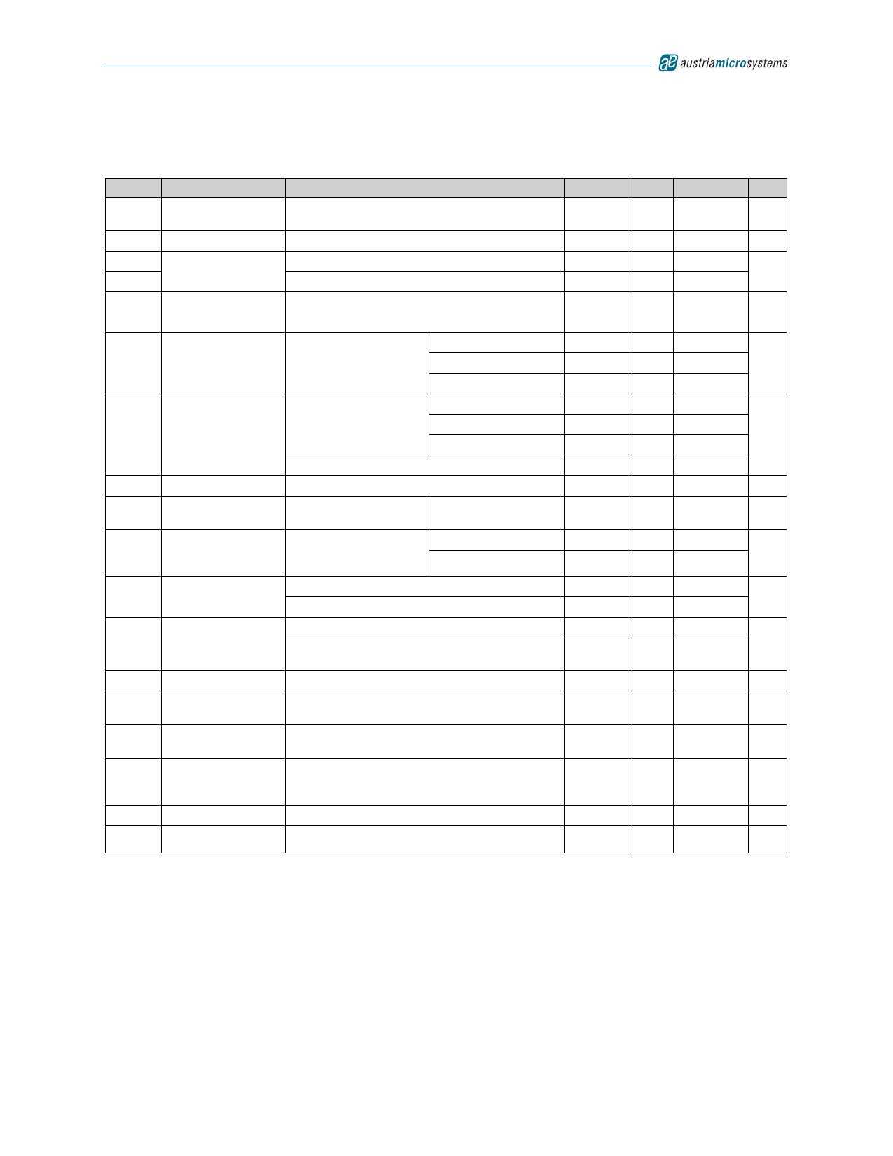
Table 5. Electrical Characteristics – 3V Supply, TAMB = +25ºC (unless otherwise specified)
Symbol
Parameter
Conditions
Min Typ
Max Unit
ICC
Supply Current 1
VIN- = VIN+ = VBIAS;
TAMB = -40 to +85ºC, per amplifier
7.5
mA
ISHDN Shutdown Supply
SHDN = SHDM = GND per amplifier
0.05
1
µA
VIH
SHDN, SHDM
VIL
Threshold
0.7 x VCC
V
0.3 x VCC
VBIAS
Common-Mode
Bias Voltage 2
VCC/2 -
5%
VCC/2 VCC/2 + 5%
V
AV = 0dB (AS1703)
VOS
Output Offset
Voltage
VIN- = VIN+ = VBIAS AV = 3dB (AS1704)
AV = 6dB (AS1705)
±1
±10
±1
±15
mV
±1
±20
AV = 0dB (AS1703)
0.2
VIC
Common-Mode
Input Voltage 3
Inferred from CMRR
Test
AV = 3dB (AS1704)
AV = 6dB (AS1705)
0.6
1.0
VCC - 0.2
VCC - 0.6
mV
VCC - 1.0
External gain AS1702
1.0
VCC - 1.0
RIN Input Impedance
AS1703, AS1704, AS1705
10
15
20
kΩ
CMRR
Common-Mode
Rejection Ratio
fN = 1kHz
-64
dB
PSRR
Power Supply
Rejection Ratio
VIN- = VIN+ = VBIAS;
VRIPPLE = 200mVp-p;
RL = 8Ω; CBIAS = 1µF
f = 217Hz
f = 1kHz
-79
dB
-73
POUT
Output Power 4
RL = 4Ω, THD+N = 1%; fIN = 1kHz
RL = 8Ω, THD+N = 1%; fIN = 1kHz
640
mW
440
Total Harmonic RL = 4Ω, fIN = 1kHz, POUT = 460mW, AV = 6dB
0.06
THD+N Distortion plus
%
Noise 5
RL = 8Ω, fIN = 1kHz, POUT = 330mW, AV = 6dB
0.04
Gain Accuracy
AS1703, AS1704, AS1705
±1
±2
%
Thermal Shutdown
Threshold
+145
ºC
Thermal Shutdown
Hysteresis
9
ºC
Power-up/Enable
tPU
from
Shutdown Time
125
ms
tSHDN Shutdown Time
3.5
µs
VPOP Turn-Off Transient 6
50
mV
1. Quiescent power supply current is specified and tested with no load. Quiescent power supply current depends on
the offset voltage when a practical load is connected to the amplifier. Guaranteed by design.
2. Common-mode bias voltage is the voltage on BIAS and is nominally VCC/2.
3. Guaranteed by design.
4. Guaranteed by design.
5. Measurement bandwidth for THD+N is 22Hz to 22kHz.
6. Peak voltage measured at power-on, power-off, into or out of SHDN. Bandwidth defined by A-weighted filters,
inputs at AC GND. VCC rise and fall times ≥ 1ms.
www.austriamicrosystems.com
Revision 1.47
5 - 20
Share Link: 