AM29LL800B Ver la hoja de datos (PDF) - Advanced Micro Devices
Número de pieza
componentes Descripción
Fabricante
AM29LL800B
Advanced Micro Devices

AM29LL800B Datasheet PDF : 40 Pages
| |||
ADVANCE INFORMATION
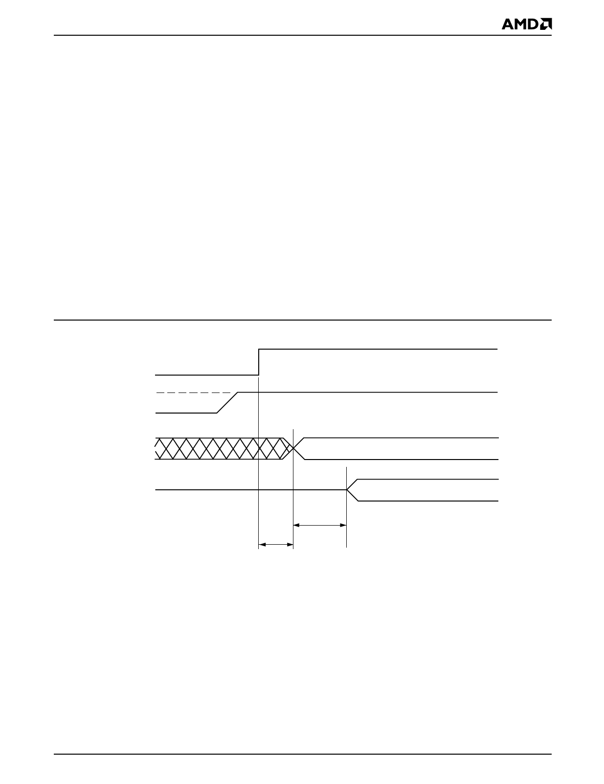
RESET#: Hardware Reset Pin
The RESET# pin provides a hardware method of reset-
ting the device to reading array data. When the RE-
SET# pin is driven low for at least a period of tRP, the
device immediately terminates any operation in
progress, tristates all output pins, and ignores all
read/write commands for the duration of the RESET#
pulse. The device also resets the internal state ma-
chine to reading array data. The operation that was in-
terrupted should be reinitiated once the device is ready
to accept another command sequence, to ensure data
integrity.
Current is reduced for the duration of the RESET#
pulse. When RESET# is held at VSS±0.3 V, the device
draws CMOS standby current (ICC4). If RESET# is held
at VIL but not within VSS±0.3 V, the standby current will
be greater.
The RESET# pin may be tied to the system reset cir-
cuitry. A system reset would thus also reset the Flash
memory, enabling the system to read the boot-up firm-
ware from the Flash memory. During power-up, the
system must ensure that RESET# is high tRSTW before
asserting a valid address (see Figure 1 and the
Erase/Program Operations table).
If RESET# is asserted during a program or erase op-
eration, the RY/BY# pin remains a “0” (busy) until the
internal reset operation is complete, which requires a
time of tREADY (during Embedded Algorithms). The
system can thus monitor RY/BY# to determine
whether the reset operation is complete. If RESET# is
asserted when a program or erase operation is not ex-
ecuting (RY/BY# pin is “1”), the reset operation is
completed within a time of tREADY (not during Embed-
ded Algorithms). The system can read data tRH after
the RESET# pin returns to VIH.
Refer to the AC Characteristics tables for RESET# pa-
rameters and to Figure 15 for the timing diagram.
Output Disable Mode
When the OE# input is at VIH, output from the device is
disabled. The output pins are placed in the high imped-
ance state.
RESET#
VCC
2.2 – 2.7 V
0V
Address
VALID
Data
tRSTW
tCE
tACC
VALID OUTPUT
Figure 1. Power-up and Reset Timings
Am29LL800B
9
Share Link: