75185-S20-T Ver la hoja de datos (PDF) - Unisonic Technologies
Número de pieza
componentes Descripción
Fabricante
75185-S20-T Datasheet PDF : 10 Pages
| |||
75185
LINEAR INTEGRATED CIRCUIT
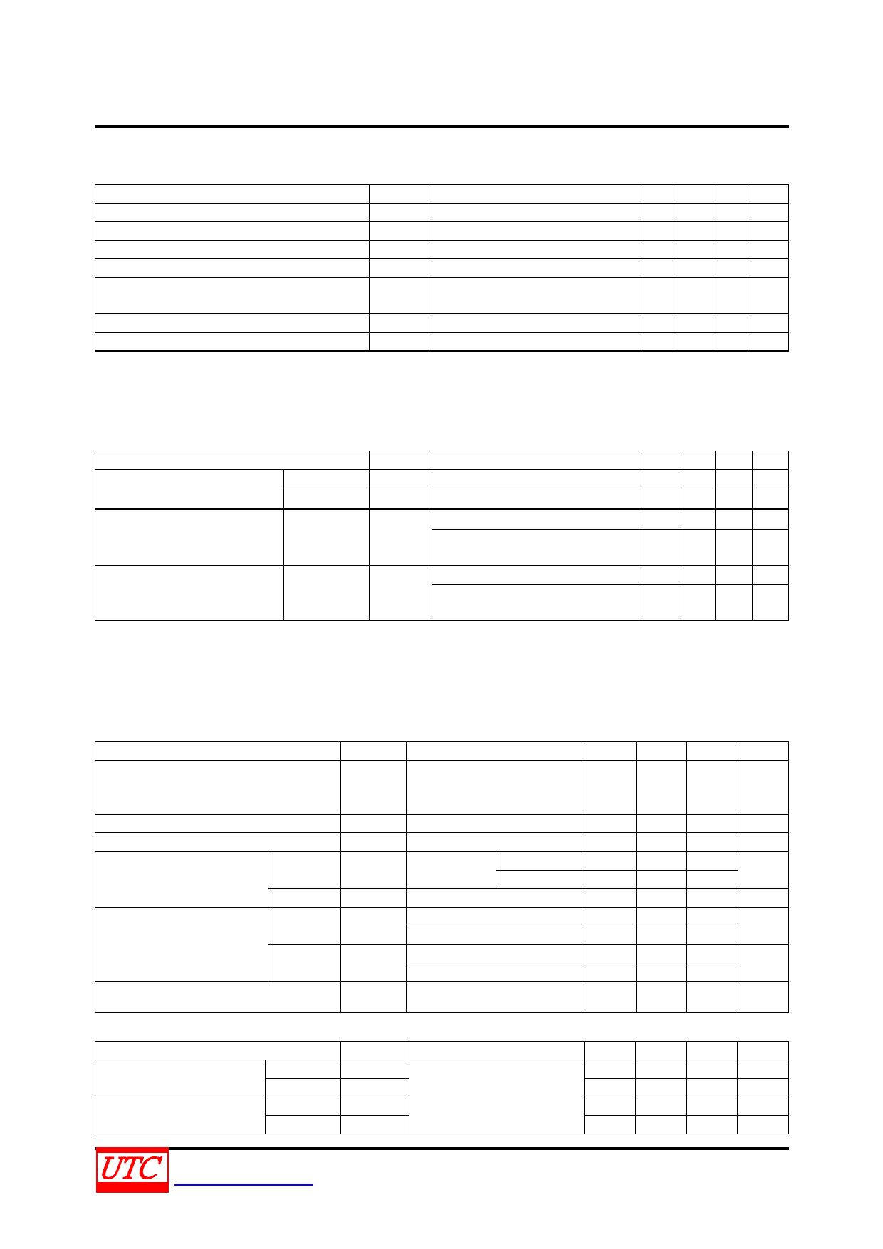
DRIVER ELECTRICAL CHARACTERISTICS OVER RECOMMENDED OPERATING
FREE-AIR TEMPERATURE RANGE (VDD=9V, VSS=-9V, VCC=5V, unless otherwise specified)
PARAMETER
SYMBOL
TEST CONDITIONS
MIN TYP MAX UNIT
High Level Output Voltage
Low Level Output Voltage (Note 3)
VOH VIL =0.8V, RL =3 kΩ (Figure 1)
VOL VIH =1.9V, RL =3 kΩ (Figure 1)
6 7.5
V
-7.5 -6 V
High Level Input Current
IIH VIN =5V (Figure 2)
10 μA
Low Level Input Current
IIL VIN =0V (Figure 2)
-1.6 mA
High Level Short Circuit Output Current
(Note 4)
IOS(H) VIL =0.8V, VOUT =0V(Figure 1)
-4.5 -12 -19.5 mA
Low Level Short Circuit Output Current
Output Resistance (Note 5)
IOS(L) VIH =2V, VOUT =0V(Figure 1)
4.5 12 19.5 mA
ROUT VDD =VSS=VCC=0V, VOUT =-2 to 2V 300
Ω
Note 3: The algebraic convention, where the more positive (less negative) limit is designated as maximum, is used in
this datasheet for logic levels only (e.g. if -10V is a maximum, the typical value is a more negative voltage).
Note 4: Output short circuit conditions must maintain the total power dissipation below absolute maximum ratings.
Note 5: Test conditions are those specified by TIA/EIA232-F and as listed above.
DRIVER SWITCHING CHARACTERISTICS (VDD=12V, VSS=-12V, VCC=5V, TA=25°C)
PARAMETER
SYMBOL
TEST CONDITIONS
MIN TYP MAX UNIT
Propagation Delay Time Level Low to High
Output
High to Low
tPLH RL=3 to 7 kΩ, CL=15pF (Figure 3)
tPHL RL=3 to 7 kΩ, CL=15pF (Figure 3)
315 500 ns
75 175 ns
RL=3 to 7 kΩ, CL=15pF (Figure 3)
60 100 ns
Transition Time Level Output Low to High
tTLH RL=3 to 7 kΩ, CL=2500pF
(Note 6,Figure 3)
1.7 2.5 μs
Transition Time Level Output High to Low
RL=3 to 7 kΩ, CL=15pF (Figure 3)
tTHL RL=3 to 7 kΩ, CL=2500pF
(Note 7, Figure 3)
40 75 ns
1.5 2.5 μs
Note 6: Measured between -3V and 3V points of the output waveform (TIA/EIA-232-F conditions), all unused inputs
are tied.
Note 7: Measured between 3V and -3V points of the output waveform (TIA/EIA-232-F conditions), all unused inputs
are tied.
RECEIVER ELECTRICAL CHARACTERISTICS OVER RECOMMENDED OPERATING
CONDITIONS (TA=25°C, VCC=5V, VDD=9V, VSS=-9V)
PARAMETER
SYMBOL TEST CONDITIONS
MIN TYP MAX UNIT
(Figure 5)
Positive Going Threshold Voltage
VT+ TA=25°C
1.75 1.9 2.3
V
TA=0°C to 70°C
1.55
2.3
Negative Going Threshold Voltage
VT-
0.75 0.97 1.25 V
Input Hysteresis (VT+ - VT-)
VHYS
0.5
V
Output Voltage
High level
VOH
IOH=-0.5mA
VIH=0.75V
Inputs Open
2.6
2.6
4
5
V
Input Current
Low level
High level
Low level
VOL VIN=3V, IOL=10mA
IIH
VIN=25V (Figure 5)
VIN=3V (Figure 5)
IIL
VIN=-25V (Figure 5)
VIN=-3V (Figure 5)
0.2 0.45 V
3.6
8.3
mA
0.43
-3.6
-0.43
-8.3 mA
Short-Circuit Output Current
IOS (Figure 4)
-3.4 -12 mA
RECEIVER SWITCHING CHARACTERISTICS (VDD=12V, VSS=-12V, VCC=5V, TA=25°C)
PARAMETER
SYMBOL TEST CONDITIONS
MIN TYP MAX
Propagation Delay Time Low to High tPLH RL=5 kΩ, CL=50pF
107 500
Level Output
High to Low tPHL (Figure 6)
42 150
Transition Time Level
Low to High tTLH
175 525
Output
High to Low tTHL
16
60
UNIT
ns
ns
ns
ns
UNISONIC TECHNOLOGIES CO., LTD
www.unisonic.com.tw
4 of 10
QW-R113-003,F
Share Link: 