5962F9563501QXC Ver la hoja de datos (PDF) - Intersil
Número de pieza
componentes Descripción
Fabricante
5962F9563501QXC Datasheet PDF : 36 Pages
| |||
HS-RTX2010RH
Input Signal, Bus, and Power Connection Descriptions (Continued)
SIGNAL
CQFP
LEAD
DESCRIPTION
EI2, EI1
8, 7 EXTERNAL INTERRUPTS 2, 1: Active HIGH level-sensitive inputs to the Interrupt Controller. Sampled on the rising
edge of PCLK. See Timing Diagrams for detail.
EI5-EI3
11-9
EXTERNAL INTERRUPTS 5, 4, 3: Dual purpose inputs; active HIGH level-sensitive Interrupt Controller inputs;
active HIGH edge-sensitive Timer/Counter inputs. As interrupt inputs, they are sampled on the rising edge of PCLK.
See Timing Diagrams for detail.
NMI
4
NON-MASKABLE INTERRUPT: Active HIGH edge-sensitive Interrupt Controller input capable of interrupting any
processor cycle when NMI is set to Mode 0. See the Interrupt Suppression and Interrupt Controller Sections.
INTSUP
5
INTERRUPT SUPPRESS: A HIGH on this pin inhibits all maskable interrupts, internal and external.
ADDRESS BUSES (OUTPUTS)
GA02
1
ASIC ADDRESS: 3-bit ASIC Address Bus, which carries address information for external ASIC devices.
GA01
84
GA00
83
MA19-MA14
56-51 MEMORY ADDRESS: 19-bit Memory Address Bus, which carries address information for Main Memory.
MA13-MA09
49-45
MA08-MA01
43-36
DATA BUSES (I/O)
GD15-GD13
17-19 ASIC DATA: 16-bit bidirectional external ASIC Data Bus, which carries data to and from off-chip I/O devices.
GD12-GD07
21-26
GD06-GD03
28-31
GD02-GD00
33-35
MD15
82 MEMORY DATA: 16-bit bidirectional Memory Data Bus, which carries data to and from Main Memory.
MD14-MD08
80-74
MD07-MD05
72-70
MD04-MD00
68-64
POWER CONNECTIONS
VDD
6, 27, Power supply +5V connections. A 0.1µF, low impedance decoupling capacitor should be placed between VDD and
50, 73 GND. This should be located as close to the RTX package as possible.
GND
20, 32,
44, 57,
69, 81
Power supply ground return connections.
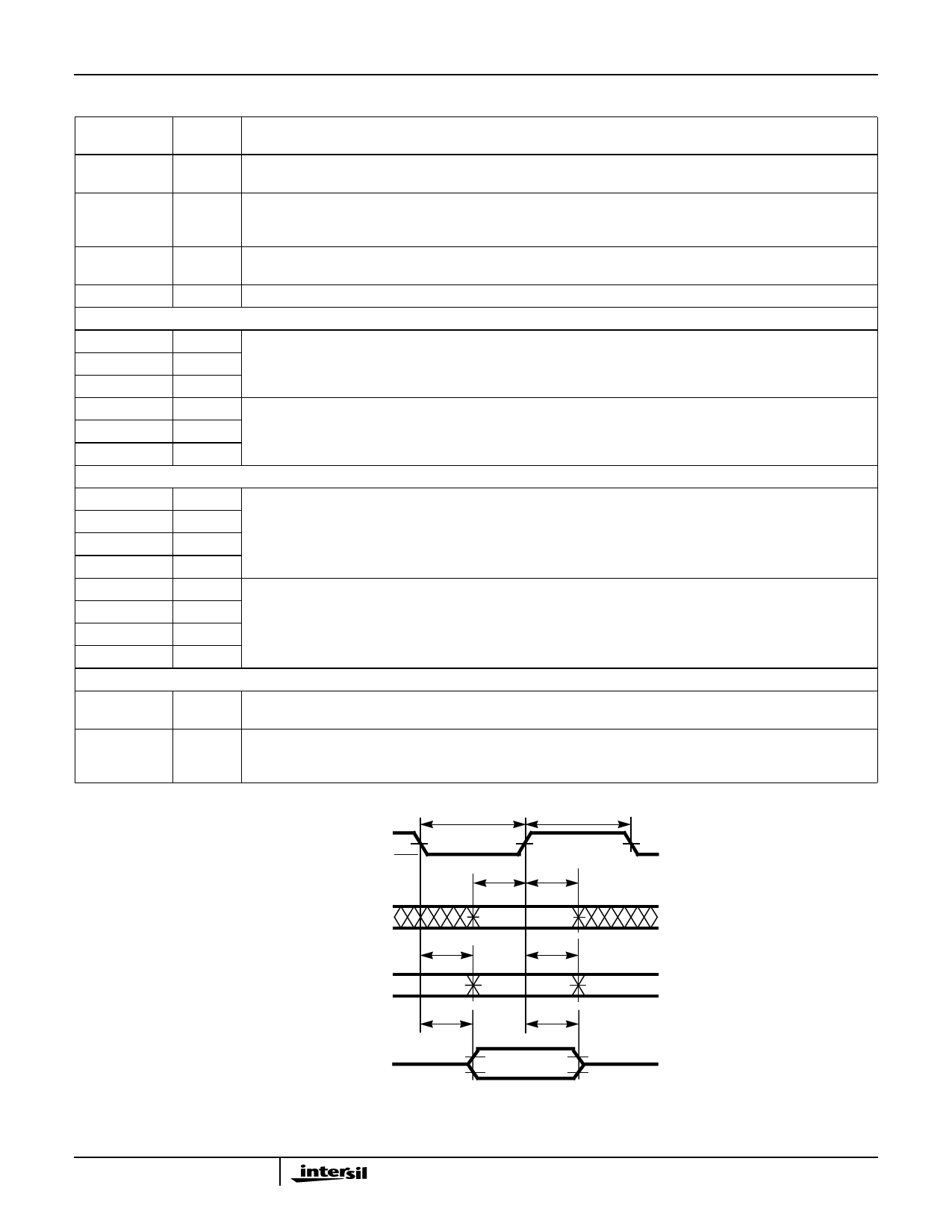
TYPICAL
CLOCK OR 4.0V
STROBE 0.5V
tPULSE WIDTH
tPULSE WIDTH
2.25V
2.25V 2.25V
tSETUP tHOLD
TYPICAL 4.0V
INPUT 0.5V
TYPICAL
OUTPUT
TYPICAL
DATA
OUTPUT
2.25V
tDELAY
2.25V
tDELAY
tVALID
2.25V
tHOLD
2.25V
2.75V 2.75V
1.75V 1.75V
FIGURE 1. AC DRIVE AND MEASURE POINTS - CLK INPUT
5
Share Link: 