27LV256 Ver la hoja de datos (PDF) - Microchip Technology
Número de pieza
componentes Descripción
Fabricante
27LV256 Datasheet PDF : 12 Pages
| |||
27LV256
1.0 ELECTRICAL
CHARACTERISTICS
1.1 Maximum Ratings*
VCC and input voltages w.r.t. VSS ........ -0.6V to +7.25V
VPP voltage w.r.t. VSS during
programming ......................................... -0.6V to +14V
Voltage on A9 w.r.t. VSS ...................... -0.6V to +13.5V
Output voltage w.r.t. VSS ............... -0.6V to VCC +1.0V
Storage temperature .......................... -65˚C to +150˚C
Ambient temp. with power applied ..... -65˚C to +125˚C
*Notice: Stresses above those listed under “Maximum Ratings”
may cause permanent damage to the device. This is a stress rat-
ing only and functional operation of the device at those or any
other conditions above those indicated in the operation listings of
this specification is not implied. Exposure to maximum rating con-
ditions for extended periods may affect device reliability.
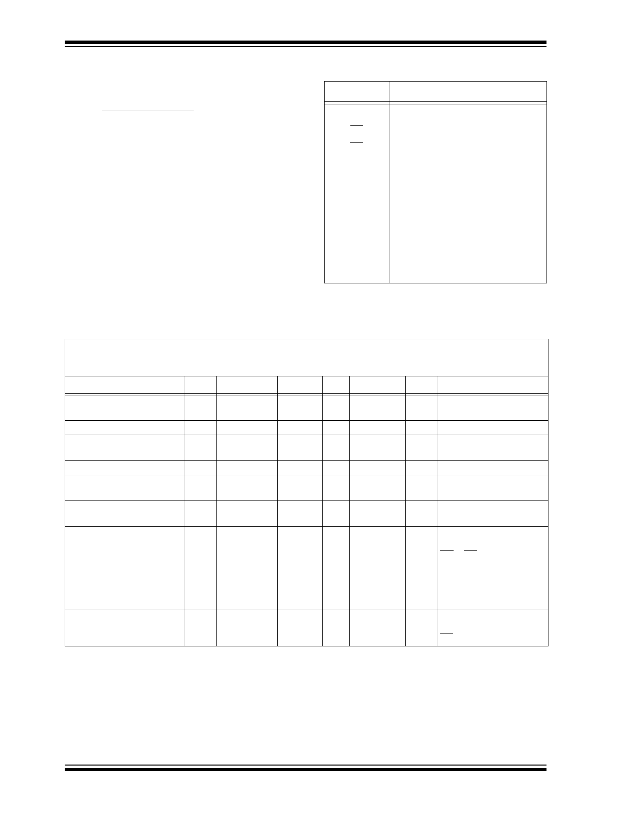
TABLE 1-1: PIN FUNCTION TABLE
Name
A0-A14
CE
OE
VPP
O0 - O7
VCC
VSS
NC
NU
Function
Address Inputs
Chip Enable
Output Enable
Programming Voltage
Data Output
+5V or +3V Power Supply
Ground
No Connection; No Internal
Connection
Not Used; No External Connection Is
Allowed
TABLE 1-2: READ OPERATION DC CHARACTERISTICS
VCC = +5V ±10% or 3.0V where indicated
Commercial:
Tamb = 0˚C to +70˚C
Industrial:
Tamb = -40˚C to +85˚C
Parameter
Part* Status Symbol Min. Max. Units
Conditions
Input Voltages
Input Leakage
Output Voltages
Output Leakage
Input Capacitance
Output Capacitance
all Logic "1"
VIH
2.0
VCC+1
V
Logic "0"
VIL -0.5
0.8
V
all
ILI
-10
10
µA VIN = 0 to VCC
all Logic "1"
Logic "0"
VOH 2.4
VOL
0.45
V IOH = -400 µA
V IOL = 2.1 mA
all
—
ILO
-10
10
µA VOUT = 0V to VCC
all
—
CIN
—
6
pF VIN = 0V; Tamb = 25°C;
f = 1 MHz
all
—
COUT —
12
pF VOUT = 0V; Tamb = 25°C;
f = 1 MHz
Power Supply Current,
Active
C
TTL input
ICC1
— 20 @ 5.0V mA VCC = 5.5V; VPP = VCC
8 @ 3.0V mA f = 1 MHz;
I
TTL input
ICC2
— 25 @ 5.0V mA OE = CE = VIL;
10 @ 3.0V mA IOUT = 0 mA;
VIL = -0.1 to 0.8V;
VIH = 2.0 to VCC;
Note 1
Power Supply Current,
Standby
C
TTL input ICC(S)
I
TTL input
all CMOS input
— 1 @ 3.0V mA
2 @ 3.0V mA
100 @ 3.0V µA CE=VCC ± 0.2V
* Parts: C=Commercial Temperature Range
I =Industrial Temperature Ranges
Note 1: Typical active current increases .75 mA per MHz up to operating frequency for all temperature ranges.
DS11020F-page 2
© 1996 Microchip Technology Inc.
Share Link: 