STV-5301-E01 Ver la hoja de datos (PDF) - Vision
Número de pieza
componentes Descripción
Fabricante
STV-5301-E01 Datasheet PDF : 51 Pages
| |||
CMOS Sensor; Customer Datasheet, Rev 3.0, 25 September 2000
VV5301 & VV6301
2. Introduction
2.1 Overview
VV5301/VV6301 is a QSIF format CMOS image sensor. The VV5301 sensor is a monochrome device and the VV6301 is the
colourised variant.
Important: The sensors’ output video data stream only contains raw data. A microprocessor and supporting software are
required to generate a video waveform that can be displayed on a VDU
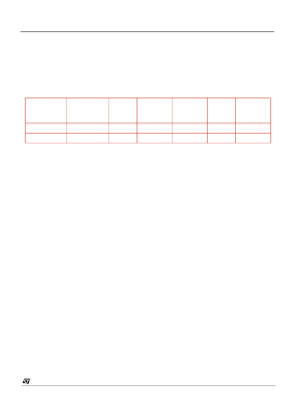
Mode
QSIF - 25 fps
QSIF - 30 fps
Input Clock
(MHz)Note
14.318
17.73
System
Clock
Divisor
1
1
Image Size
164 x 124
164 x 124
Line Time
(µs)
271.502
227.36
Lines
per
Frame
147
147
Frame Rate
(fps)
25.06
29.92
VV5301/VV6301 have an on-board 8bit ADC, this limits the number of components required to form a complete digital imaging
system.
The VV5301/VV6301 sensor will output an image size of 164 x 124. This is an oversized QSIF image. The extra pixels that the
form the 2 pixel deep border that surrounds the true QSIF image are made available to the external colour processing algorithm.
2.2 Exposure, Clock Division and Gain Control
VV5301/VV6301 have an internal automatic exposure/gain control algorithm. This algorithm can be disabled allowing the user to
externally control the exposure. The externally calculated exposure, clock division and gain control settings would then be written
to the sensor via the I2C interface.
2.3 Digital Interface
VV5301/VV6301 have a flexible digital interface, the main components of which are listed below:
1. A tri-stateable 8-wire data bus (D[7:0]) for sending both video data and embedded timing references.
2. 4-wire and 8-wire data bus alternatives available.
3. A data qualification clock, QCK, which can be programmable via the serial interface to behave in a number of different ways
(Tri-stateable).
4. A line start signal, LST (Tri-stateable).
5. A frame start signal, FST (Tri-stateable).
6. OEB tri-states all 5 data bus lines, D[4:0], the qualification clock, QCK and FST.
7. The ability to synchronise the operation of multiple cameras (sensor produces a synchronisation out pulse, SNO).
8. A 2-wire serial interface (SDA,SCL) for controlling and setting up the device.
2.3.1 Digital Data Bus
Along with the pixel data, codes representing the start and end of fields and the start and end of lines are embedded within the
video data stream to allow a co-processor to synchronise with video data the camera module is generating Section 7.defines the
format for the output video data stream.
2.3.2 Frame Grabber Control Signals
To complement the embedded control sequences the data qualification clock (QCK) and the field start signal (FST) signals can
be independently set-up as follows:
1. Disabled
2. Free-running.
3. Qualify only the control sequences and the pixel data.
4. Qualify the pixel data only
cd5301_6301f-3-0.fm
5/50
Commercial in confidence
Share Link: 