IMP527D1 Ver la hoja de datos (PDF) - IMP, Inc
Número de pieza
componentes Descripción
Fabricante
IMP527D1 Datasheet PDF : 8 Pages
| |||
IMP527
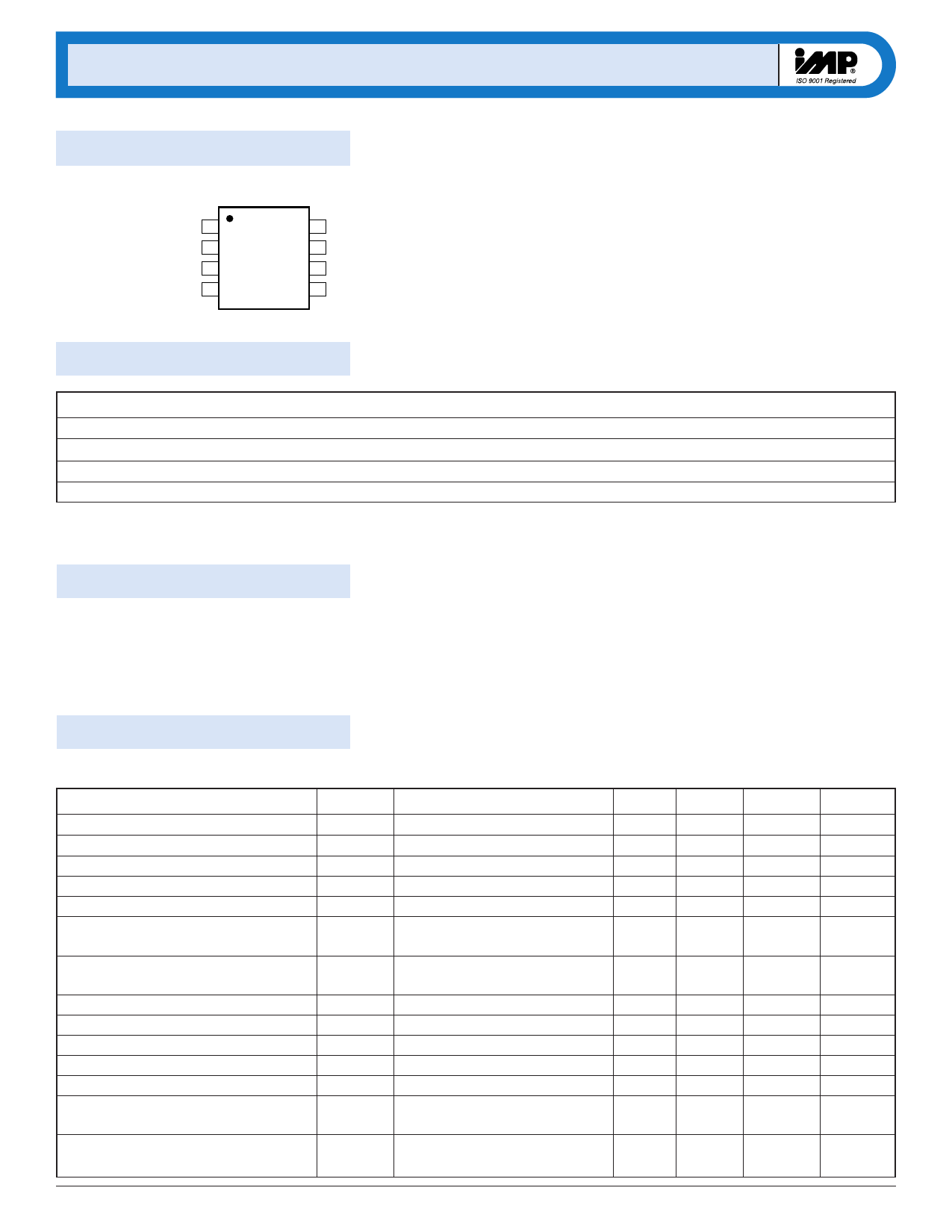
Pin Configuration
SO/MicroSO
VDD 1
RSW-OSC 2
CS 3
LX 4
IMP527
8 REL-OSC
7 VA
6 VB
5 GND
527_02.eps
Ordering Information
Part Number Input Voltage
IMP527EMA
0.9V to 2.5V
IMP527ESA
0.9V to 2.5V
IMP527/D*
0.9V to 2.5V
IMP527/D1**
0.9V to 2.5V
* Disable pad not active
** Disable pad active
Regulated Output Voltage
YES
YES
YES
YES
Temperature Range
– 40°C to +85°C
– 40°C to +85°C
25°C
25°C
Pins-Package
8-MicroSO
8-SO
Dice
Dice
Absolute Maximum Ratings
Supply Voltage, VDD, VRSW-OSC and VREL-OSC . . – 0.5V to +3.5V
Storage Temperature Range . . . . . . . . . . . . . . . . – 65°C to +150°C
Power Dissipation (SO package) . . . . . . . . . . . . 400mW
Power Dissipation (MicroSO package) . . . . . . . 300mW
Note: All voltages are referenced to GND.
These are stress ratings only and functional operation is not implied.
Exposure to absolute maximum ratings for prolonged time periods may
affect device reliability.
Electrical Characteristics
Unless otherwise noted, VDD = 1.5V, RSW = 1MΩ, REL = 1MΩ, and TA = 25°C.
Parameter
ON-resistance of MOS Switch
Operating Voltage
Output Voltage at CS
Output Voltage at CS
Output Voltage Peak-to-Peak
Quiescent VDD Supply Current, Disabled
(Disable pin available on die only)
Quiescent VDD Supply Current, Disabled
Input Current at VDD Pin
Input Current: IDD Plus Inductor Current
VA-B Output Drive Frequency
Boost Converter Switching Frequency
Switching Duty Cycle
Disable Input LOW Voltage
(Disable pin available on die only)
Disable Input HIGH Voltage
(Disable pin available on die only)
Symbol Conditions
RDS(ON) I = 50mA
VCS
VCS
VA-VB
IQDIS
VDD = 1.5V, See Figure 1, Table 1
VDD = 0.9V, See Figure 1, Table 2
VDD = 1.5V, See Figure 1
Disable = HIGH
Min
0.9
80
IQDIS
IDD
IIN
fEL
fSW
DSW
VDISL
RSW-OSC = GND
VDD = 1.5V
VDD = 0.9V to 1.5V
VDD = 1.5V, See Figure 1, Table 1
VDD = 1.5V, See Figure 1, Table 1
VDD = 1.5V, See Figure 1, Table 1
VDD = 1.5V, See Figure 1
GND
VDISH
VDD -0.5V
Typ
90
50
180
70
1.0
26
500
26
87.5
2
408-432-9100/www.impweb.com
Max
15
2.5
2.0
1.5
32
0.2
VDD
Units
Ω
V
V
V
VP-P
nA
µA
mA
mA
Hz
kHz
%
V
V
© 2000 IMP, Inc.
Share Link: 