AWT1921 Ver la hoja de datos (PDF) - ANADIGICS
Número de pieza
componentes Descripción
Fabricante
AWT1921 Datasheet PDF : 12 Pages
| |||
AWT1921
VD3
VD2
VD1
VDD/VREF
VG4
VSS
VD4
GND
6
F3
C1
C4
F2
C3
F1
C5
RFIN
C11
L5
C23
R4
R3
C7
AWT1921S11
C10
10
9 VD3
4 VD2
3
2
VD1
RFIN/VGS1
5
R5
6 GND
7
8
C12
C13
26 VREF
27 VDD
13 VG3 GND
25
24
23
VD4
22
21
20
19
18
VGS2
VSS
11
12
VGS4 16
17
C15
C14
C18
R2
C16
C17
F5
C19
RFOUT
C20
C21
F4
C22
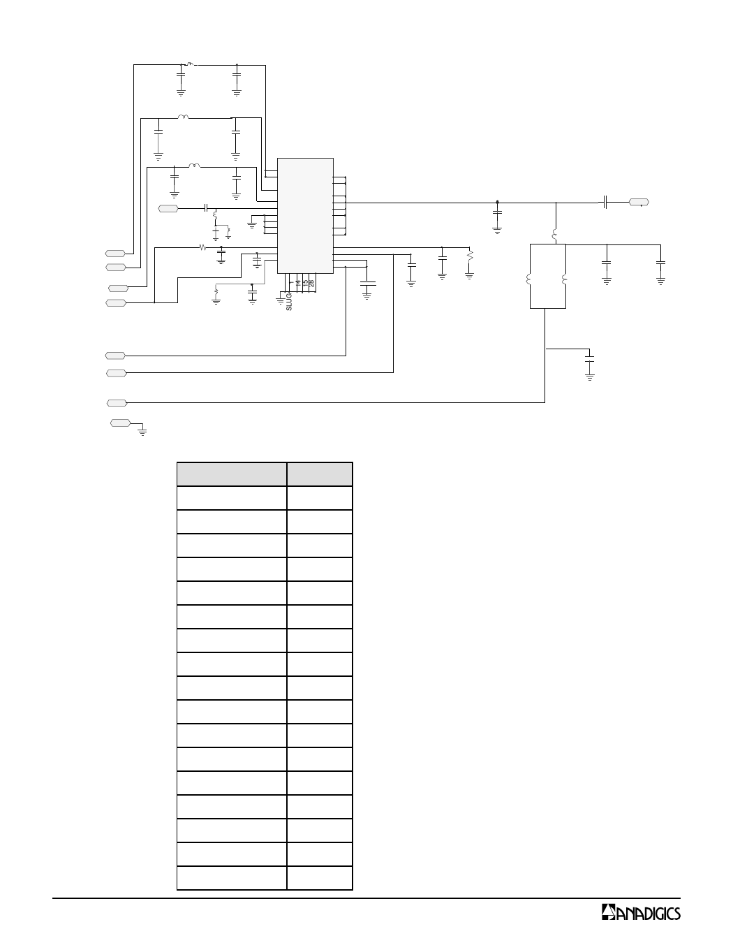
Figure 10: 1610 - 1626.5 MHz Test Circuit Schematic
Table 4: Pin Designations
DESIGNATION
VALUE
C1,C3,C5,C22
2.2 F
C2,C7,C9,C24
Not Used
C4
15 pF
C6, C10
10 pF
C11,C19
27 pF
C12,C13,C20,C21 33 pF
C14,C16,C17,C23 0.01 uF
C15
22 pF
C18
4.7 pF
F1,F2,F3,F4,F5
Feritte
L1,L3
Shim
L2
2.7 nH
L4
8 nH
L5
47 nH
R2, R5
5600
R3
1500
R4
2200
Procedure for Amplifier Operation and Test
1) Slug must be thermally and electrically connected
to obtain rated performance.
2) The VSS voltage should be applied first to the
amplifier prior to VD1, VD2, VD3, or VD4 voltages.
3) VGS1, VGS2, VGS3, VGS4 may be used as monitor points
to verify that the bias circuit is working properly. These
pins should measure as negative voltage potential,
after VSS is applied.
4) The Bias Pins VDD and VREF may be applied with no
VSS voltage present.
5) Always follow ESD precautions when handling
these devices.
PRELIMINARY DATA SHEET - Rev 1.0
08/2001
Share Link: 