ATA01504D1C Ver la hoja de datos (PDF) - ANADIGICS
Número de pieza
componentes Descripción
Fabricante
ATA01504D1C Datasheet PDF : 8 Pages
| |||
IIN connection
(refer to the equivalent circuit diagram) Bonding the
detector cathode to IIN (and thus drawing current from
the ATA01504) improves the dynamic range. Although
the detector may be used in the reverse direction for
input currents not exceeding 25 mA, the specifications
for optical overload will not be met.
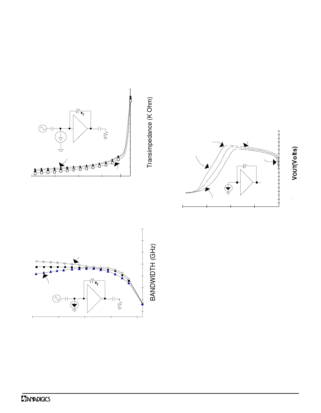
10
9
8
7
I IIN
6
50
5
4
VDD = 5.5 V
3
VDD = 4.5 V 2
-2.1 - 1.6 -1.1 - 0.6 - 0.1 1
IIN (mA DC)
Figure 5: Transimpedance vs. IIN
ATA01504
VOUT Connection
The output pad should be connected via a coupling
capacitor to the next stage of the receiver channel
(filter or decision circuits), as the output buffers are
not designed to drive a DC coupled 50 ohm load
(this would require an output bias current of
approximately 36 mA to maintain a quiescent 1.8
Volts across the output load). If VOUT is connected to a
high input impedance decision circuit (>500 ohms),
then a coupling capacitor may not be required,
although caution should be exercised since DC
offsets of the photo detector/TIA combination may
cause clipping of subsequent gain or decision
circuits.
3.4
Output Collapse
heavy AGC 3.2
3.0
2.9
2.7
2.5
VDD =5.5 V
Linear Region
2.4
2.2
2.0
1.9
1.7
Rf
1.5
1.4
IIN
1.2
VOUT 1.0
0.8
0.7
0.5
0.3
VDD = 4.5 V
0.2
0.0
-4
-3
-2
-1
Bandwidth vs IIN
1.5
1.3
VDD=5.5 V
1.1
0.9
VDD=4.5 V
1501
IIN
0.7
0.5
50 0.3
0.1
- 2.1 - 1.6 - 1.1 - 0.6 - 0.1
IIN (mA DC)
IIN (mA DC)
Figure 7: VOUT vs. IIN
Sensitivity and Bandwidth
In order to guarantee sensitivity and bandwidth
performance, the TIA is subjected to a
comprehensive series of tests at the die sort level
(100% testing at 25 oC) to verify the DC parametric
performance and the high frequency performance
(i.e. adequate |S21|) of the amplifier. Acceptably high
|S21| of the internal gain stages will ensure low
amplifier input capacitance and hence low input
referred noise current. Transimpedance sensitivity
and bandwidth are then guaranteed by design and
correlation with RF and DC die sort test results.
Figure 6: Bandwidth vs. IIN
PRELIMINARY DATA SHEET - Rev 1
5
08/2001
Share Link: 