FS612509-01 Ver la hoja de datos (PDF) - AMI Semiconductor
Número de pieza
componentes Descripción
Fabricante
FS612509-01 Datasheet PDF : 9 Pages
| |||
FS612509-01/-02
1:9 Zero-Delay Clock Buffer IC
1.0 Features
• Generates one bank of five outputs (1Y0 to 1Y4) and
one bank of four outputs (2Y0 to 2Y3) from one ref-
erence clock input (CLK)
• Designed to meet the PLL Component Specifications
as noted in the PC133 SDRAM Registered DIMM
Design Specification
• External feedback input (FBIN) to synchronize all
clock outputs to the clock input
• Operating frequency: 25MHz to 140MHz
• Tight tracking skew (spread-spectrum tolerant)
• On-chip 25Ω series damping resistors for driving
point-to-point loads
• Separate bank controls:
M Signal 1G enables or disables outputs 1Y0 - 1Y4
M Signal 2G enables or disables outputs 2Y0 - 2Y3
• Available with an auto power-down option that turns
off the PLL and forces all outputs low when the refer-
ence clock stops (FS612509-02)
• Packaged in a 24-pin TSSOP
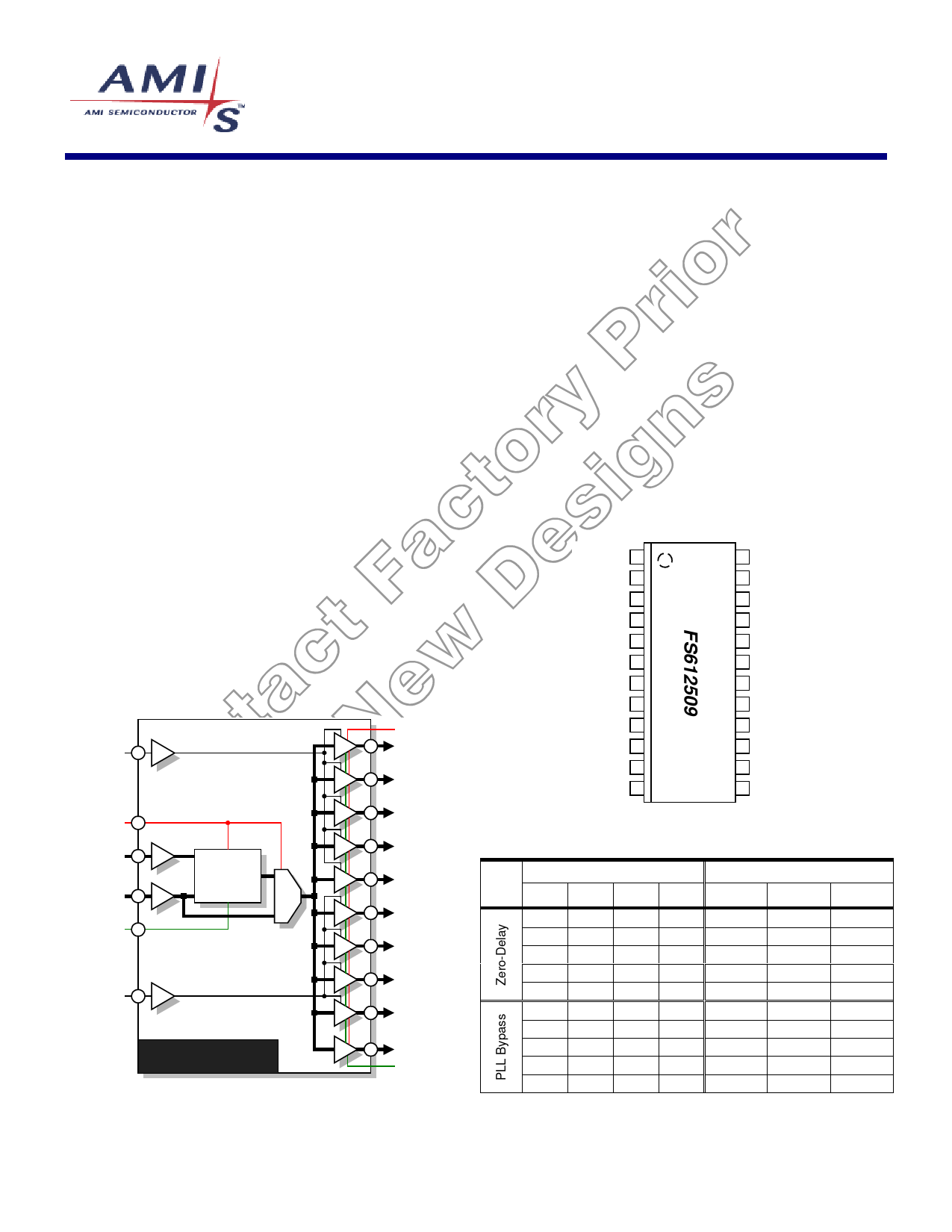
Figure 1: Block Diagram
1G
AVDD
FBIN
CLK
AGND
PLL
2G
FS612509
VDD
1Y0
1Y1
1Y2
1Y3
1Y4
2Y0
2Y1
2Y2
2Y3
FBOUT
GND
2.0 Description
The FS612509 is a low skew, low jitter CMOS zero-delay
phase-lock loop (PLL) clock buffer IC designed for high-
speed motherboard applications, such as those using
133MHz SDRAM.
Nine buffered clock outputs are derived from an onboard
open-loop PLL. The PLL aligns the frequency and phase
of all output clocks to the input clock CLK, including an
FBOUT clock that feeds back to FBIN to close the loop.
One group of five outputs 1Y0 to 1Y4 are enabled and
disabled low by the active-high 1G signal. A second
group of four outputs 2Y0 to 2Y3 are enabled and dis-
abled low by the active-high 2G signal. The PLL may be
bypassed by pulling AVDD to ground.
Figure 2: Pin Configuration
AGND 1
VDD 2
1Y0 3
1Y1 4
1Y2 5
GND 6
GND 7
1Y3 8
1Y4 9
VDD 10
1G 11
FBOUT 12
24 CLK
23 AVDD
22 VDD
21 2Y0
20 2Y1
19 GND
18 GND
17 2Y2
16 2Y3
15 VDD
14 2G
13 FBIN
Table 1: Function Table
PLL
AVDD
H
H
H
H
H
L
L
L
L
L
INPUT
1G 2G
L
L
L
H
H
L
H
H
H
H
L
L
L
H
H
L
H
H
H
H
OUTPUT
CLK 1Y0-1Y4 2Y0-2Y3 FBOUT
H
L
L
H
H
L
H
H
H
H
L
H
H
H
H
H
L
L
L
L
H
L
L
H
H
L
H
H
H
H
L
H
H
H
H
H
L
L
L
L
This document contains information on a new product. Specifications and information herein are subject to change without notice.
ISO9001
QS9000
3.1.02
Share Link: 