AFBR-5803Z Ver la hoja de datos (PDF) - Avago Technologies
Número de pieza
componentes Descripción
Fabricante
AFBR-5803Z
Avago Technologies

AFBR-5803Z Datasheet PDF : 16 Pages
| |||
Solder and Wash Process Compatibility
The transceivers are delivered with protective process
plugs inserted into the duplex SC or duplex ST connector
receptacle. This process plug protects the optical subas-
semblies during wave solder and aqueous wash process-
ing and acts as a dust cover during shipping.
These transceivers are compatible with either industry
standard wave or hand solder processes.
Shipping Container
The transceiver is packaged in a shipping container
designed to protect it from mechanical and ESD damage
during shipment or storage.
Board Layout - Decoupling Circuit and Ground Planes
It is important to take care in the layout of your circuit
board to achieve optimum performance from these
transceivers. Figure 7 provides a good example of a
schematic for a power supply decoupling circuit that
works well with these parts. It is further recommended
that a contiguous ground plane be provided in the
circuit board directly under the transceiver to provide
a low inductance ground for signal return current. This
recommendation is in keeping with good high frequency
board layout practices.
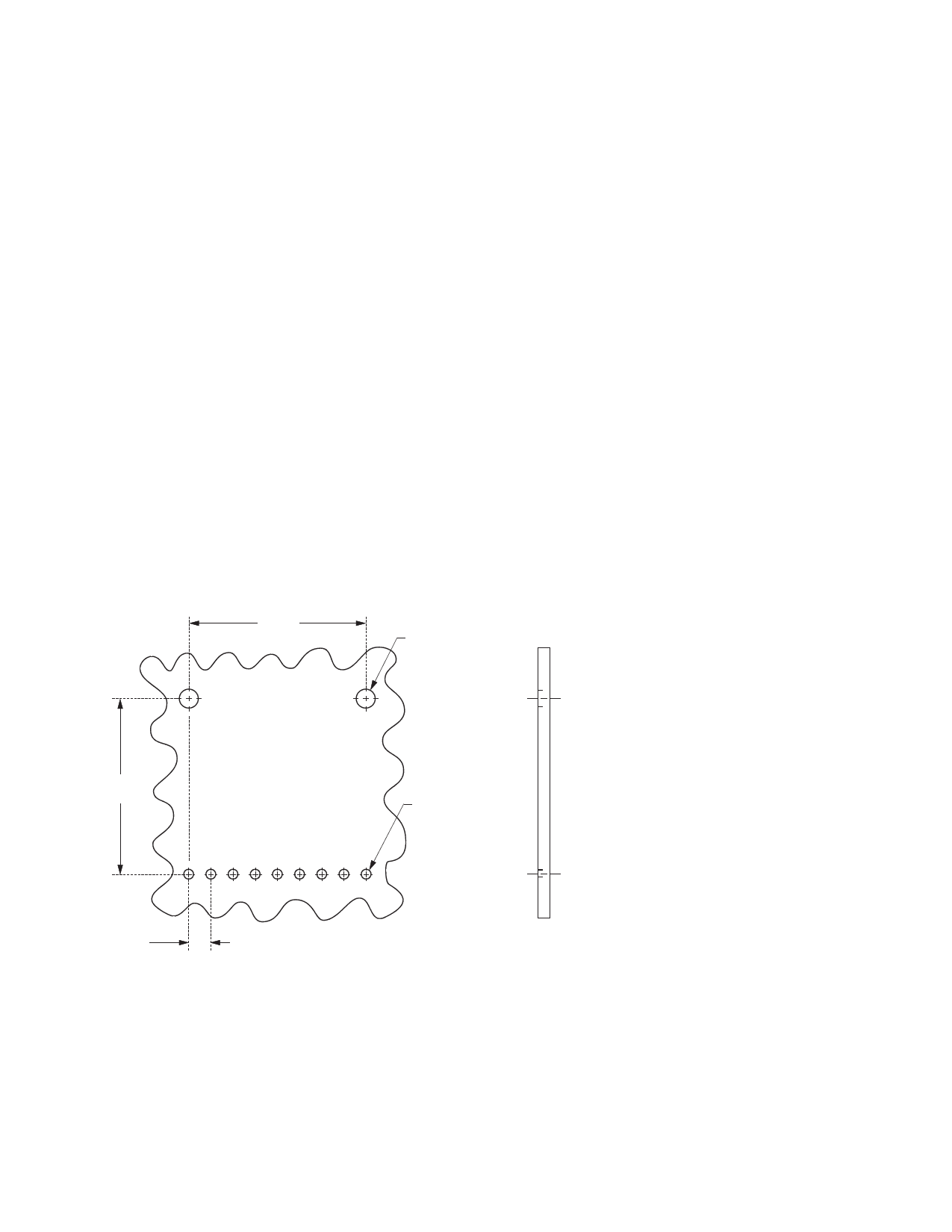
Board Layout - Hole Pattern
The Avago Technologies transceiver complies with the
circuit board “Common Transceiver Footprint” hole
pattern defined in the original multisource announce
ment which defined the 1 x 9 package style. This drawing
is reproduced in Figure 8 with the addition of ANSI
Y14.5M compliant dimensioning to be used as a guide in
the mechanical layout of your circuit board.
Board Layout - Mechanical
For applications providing a choice of either a duplex SC
or a duplex ST connector interface, while utilizing the
same pinout on the printed circuit board, the ST port
needs to protrude from the chassis panel a minimum
of 9.53 mm for sufficient clearance to install the ST
connector.
Please refer to Figure 8a for a mechanical layout detailing
the recommended location of the duplex SC and duplex
ST transceiver packages in relation to the chassis panel.
20.32
(0.800)
2 x Ø 1.9 ± 0.1
(0.075 ± 0.004)
20.32
(0.800)
9 x Ø 0.8 ± 0.1
(0.032 ± 0.004)
2.54
(0.100)
TOP VIEW
DIMENSIONS ARE IN MILLIMETERS (INCHES)
Figure 8. Recommended Board Layout Hole Pattern
Share Link: