TA2021B Ver la hoja de datos (PDF) - Tripath Technology Inc.
Número de pieza
componentes Descripción
Fabricante
TA2021B
Tripath Technology Inc.

TA2021B Datasheet PDF : 12 Pages
| |||
Tripath Technology, Inc. - Technical Information
Application Information
Circuit Board Layout
The TA2021B is a power amplifier which operates at relatively high switching frequencies. The
outputs of the amplifier switch between VDD and PGND at frequencies as high as 1MHz while
driving high currents. This high-frequency digital signal is passed through an LC low-pass filter to
recover the amplified audio signal. Because the TA2021B drives the inductive LC output filters
and speaker load, the amplifier outputs can be pulled above VDD and below PGND by the stored
energy in the output inductance. To avoid subjecting the TA2021B to potentially damaging
voltage stress, it is critical to have a good printed circuit board layout to minimize parasitic effects
caused by excessive trace inductance/capacitance. It is recommended that Tripath’s layout and
application circuit be used as closely as possible for all applications and only be deviated from
after careful analysis of the effects of any changes.
Output Stage layout Considerations and Component Selection Criteria
Proper PCB layout and component selection is a major step in designing a reliable TA2021B
power amplifier. The supply pins require proper decoupling with correctly chosen components to
achieve optimal reliability. The output pins need proper protection to keep the outputs from going
below ground and above VDD.
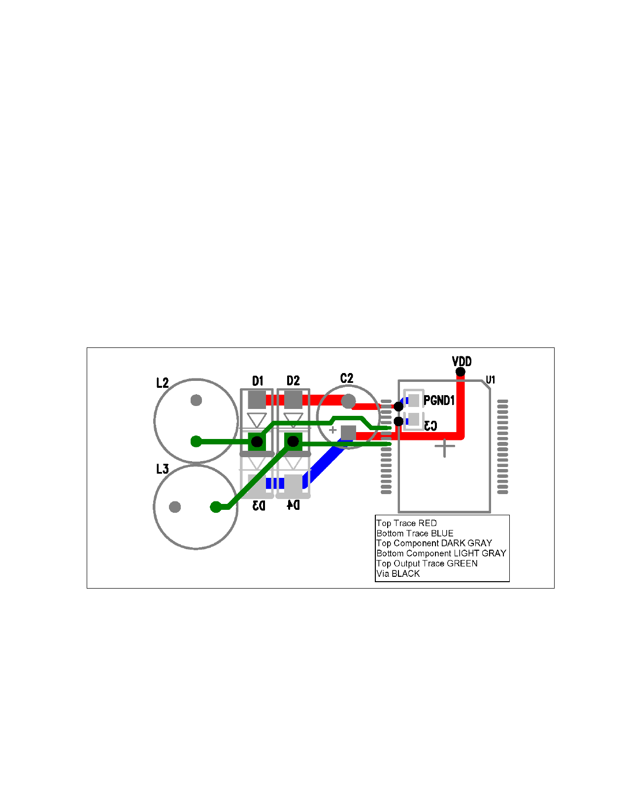
The above layout shows component placement and routing for channel 1 (the same design
criteria applies to channel 2). This shows that C3, a 0.1uF surface mount 0805 capacitor, should
be the first component placed and must decouple VDD1 (pins 29 and 30) directly to PGND1
(pin35). C2, a low ESR, electrolytic capacitor, should also decouple VDD1 directly to PGND1.
Both C2 and C3 may decouple VDD1 to a ground plane, but it is critical that the return path to the
PGND1 pin of the TA2021B, whether it is a ground plane or a trace, be a short and direct low
impedance path. Effectively decoupling VDD will shunt any power supply trace length inductance.
The diodes and inductors shown are for channel 1’s outputs. D1, D3, and L2 connect to the
OUTP1 pin and D2, D4, and L3 connect to the OUTM1 pin of the TA2021B. Each output must
have Schottky or Ultra Fast Recovery diodes placed near the TA2021B, preferably immediately
8
TA2021B – 3.0/04.03
Share Link: