RDA1846 Ver la hoja de datos (PDF) - Unspecified
Número de pieza
componentes Descripción
Fabricante
RDA1846 Datasheet PDF : 16 Pages
| |||
RDA Microelectronics, Inc.
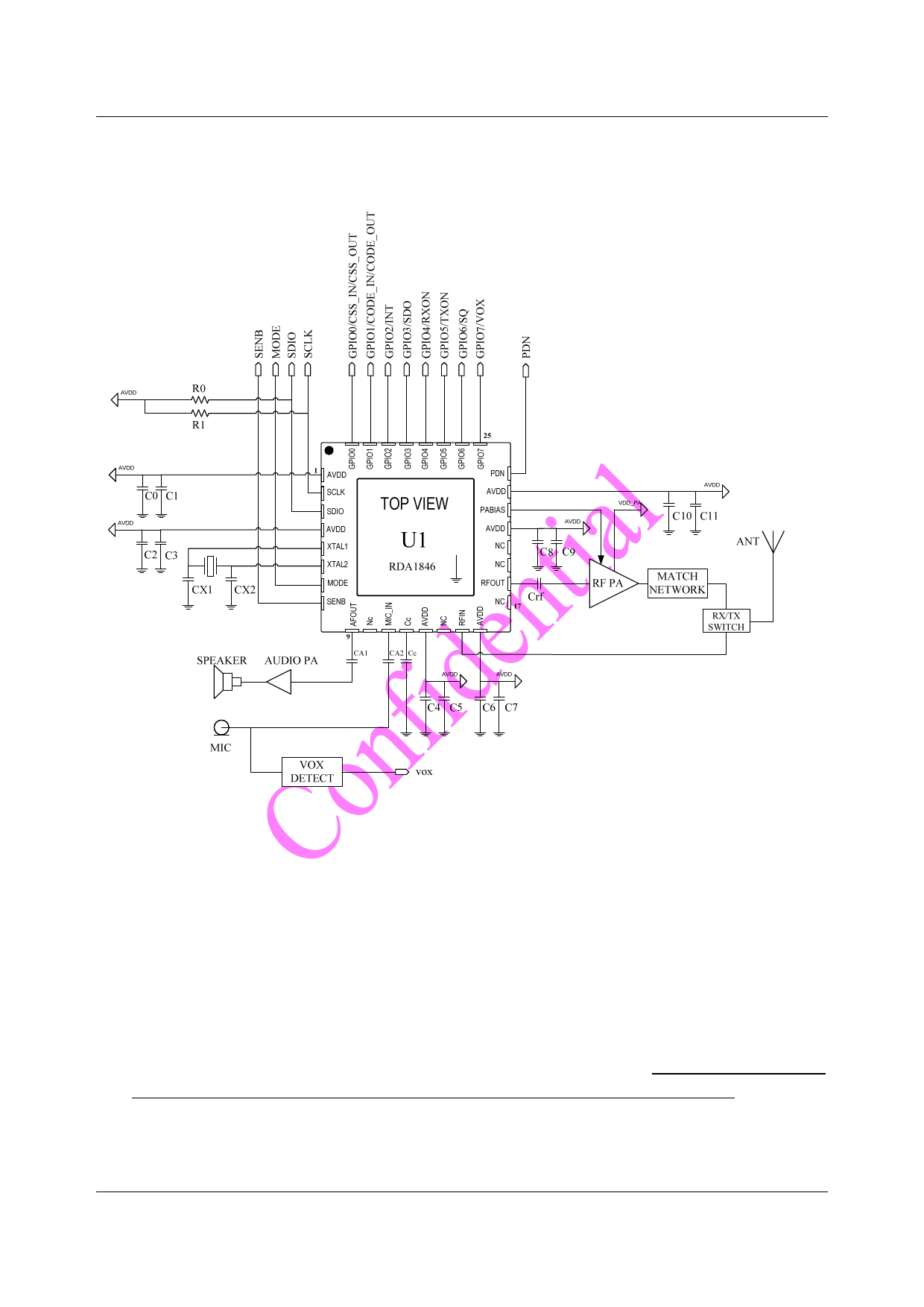
8. Application Diagram
RDA1846 SPEC V1.2e
Figure 8.1 RDA1846 Application Diagram
Notes:
1 U1: RDA1846 Chip;
2 AVDD: Power Supply for RDA1846 (3.3~4.8V);
3 AVDD_PA: Power Supply for RF PA, its voltage depends on the actual PA design;
4 C0~C11: AVDD decouple capacitance (1nF and 100nF in pairs), as close to AVDD pin as possible;
5 CA1~CA2: Audio AC couple capacitance (~47uF);
6 Cc: Compensation capacitance connected between pin Cc and GND (~47uF);
7 Crf: RF AC couple capacitance (~150pF);
8 CX1~CX2: XTAL oscillator load capacitance. Its value depends on the chosen XTAL (if using external TCXO, clk
should be sent into pin XTAL1 with Vpp about 1.5V, and pin XTAL2 should be connected to GND);
9 R0~R1(optional): resistors for serial interface wire SDIO and SCLK (~10kΩ);
10 Pins NC(10,14,17,19,20) should be floating;
11 External vox detection circuit is optional;
The information contained herein is the exclusive property of RDA and shall not be distributed, reproduced, or disclosed in whole or in
part without prior written permission of RDA.
Page 11 of 16
Share Link: 