MAX9945 Ver la hoja de datos (PDF) - Unspecified
Número de pieza
componentes Descripción
Fabricante
MAX9945 Datasheet PDF : 13 Pages
| |||
38V, Low-Noise, MOS-Input,
Low-Power Op Amp
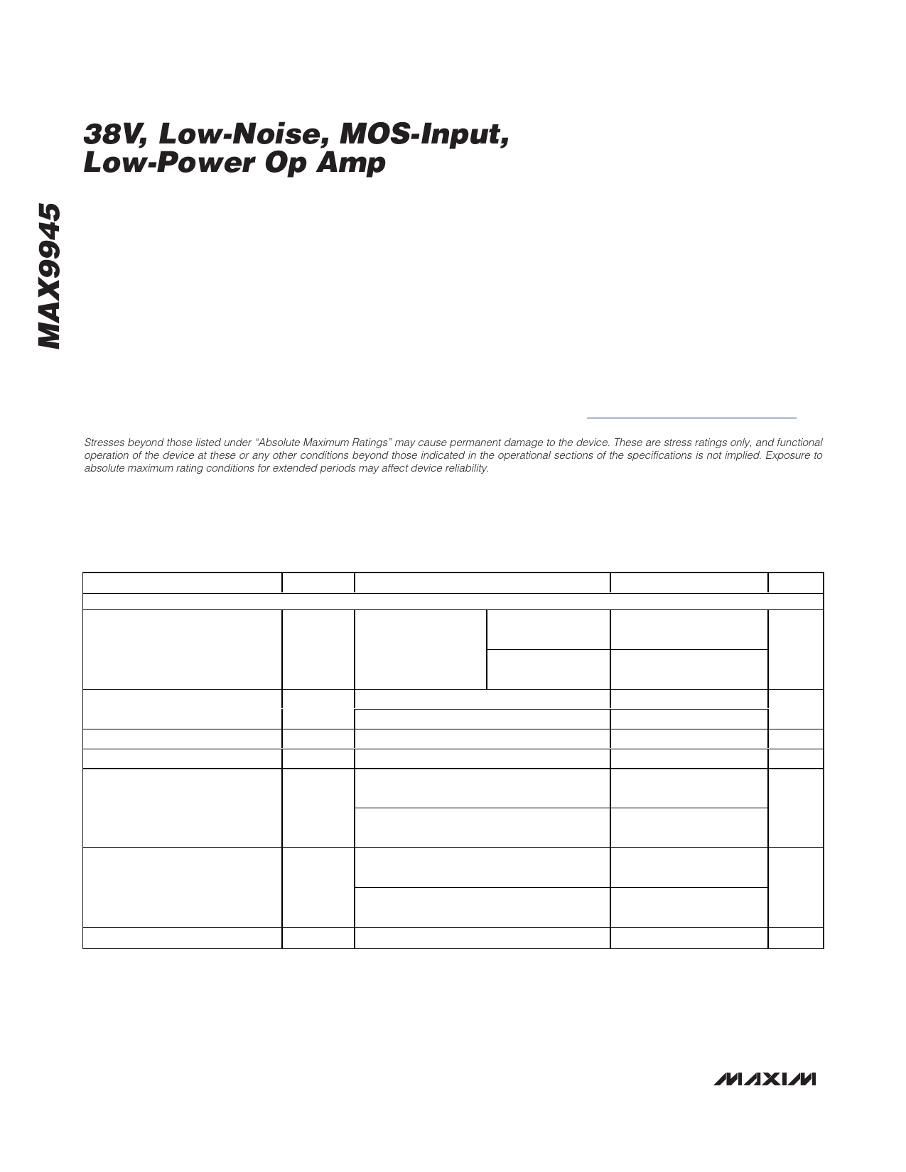
ABSOLUTE MAXIMUM RATINGS
Supply Voltage (VCC to VEE) ..................................-0.3V to +40V
IN+, IN-, OUT Voltage......................(VEE - 0.3V) to (VCC + 0.3V)
IN+ to IN- .............................................................................±12V
OUT Short Circuit to Ground Duration....................................10s
Continuous Input Current into Any Pin .............................±20mA
Continuous Power Dissipation (TA = +70°C)
6-Pin TDFN-EP (derate 23.8mW/°C above +70°C)
Multilayer Board ....................................................1904.8mW
Package Thermal Resistance (Note 1)
θJA ..............................................................................42°C/W
θJC................................................................................9°C/W
8-Pin µMAX (derate 4.8mW/°C above +70°C)
Multilayer Board ......................................................387.8mW
Package Thermal Resistance (Note 1)
θJA .........................................................................206.3°C/W
θJC..............................................................................42°C/W
Operating Temperature Range .........................-40°C to +125°C
Junction Temperature ......................................................+150°C
Storage Temperature Range .............................-65°C to +150°C
Lead Temperature (soldering, 10s) .................................+300°C
Note 1: Package thermal resistances were obtained using the method described in JEDEC specification JESD51-7, using a four-
layer board. For detailed information on package thermal considerations, refer to www.maxim-ic.com/thermal-tutorial.
Stresses beyond those listed under “Absolute Maximum Ratings” may cause permanent damage to the device. These are stress ratings only, and functional
operation of the device at these or any other conditions beyond those indicated in the operational sections of the specifications is not implied. Exposure to
absolute maximum rating conditions for extended periods may affect device reliability.
ELECTRICAL CHARACTERISTICS
(VCC = +15V, VEE = -15V, VIN+ = VIN- = GND = 0, ROUT = 100kΩ to GND, TA = -40°C to +125°C, typical values are at TA = +25°C,
unless otherwise noted.) (Note 2)
PARAMETER
SYMBOL
DC ELECTRICAL CHARACTERISTICS
CONDITIONS
Input Voltage Range
VIN+, VIN-
Guaranteed by
CMRR
TA = +25°C
TA = TMIN to TMAX
Input Offset Voltage
Input Offset Voltage Drift
Input Bias Current (Note 3)
Common-Mode Rejection Ratio
Open-Loop Gain
Output Short-Circuit Current
VOS
VOS - TC
IB
CMRR
AOL
ISC
TA = +25°C
TA = TMIN to TMAX
VCM = VEE to VCC - 1.2V,
TA = +25°C
VCM = VEE to VCC - 1.4V,
TA = TMIN to TMAX
VEE + 0.3V ≤ VOUT ≤ VCC - 0.3V,
ROUT = 100kΩ to GND
VEE + 0.75V ≤ VOUT ≤ VCC - 0.75V,
ROUT = 10kΩ to GND
MIN TYP MAX UNITS
VEE
VCC -
1.2
V
VEE
VCC -
1.4
±0.6
±5
mV
±8
2
µV/°C
50
fA
78
94
dB
78
94
110 130
dB
110 130
25
mA
2 _______________________________________________________________________________________
Share Link: 