LD7535A Ver la hoja de datos (PDF) - Unspecified
Número de pieza
componentes Descripción
Fabricante
LD7535A Datasheet PDF : 19 Pages
| |||
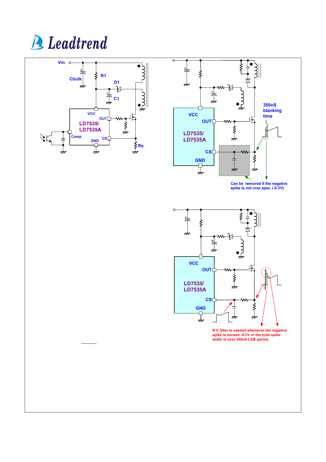
LD7535/LD7535A
Fig. 15
A 350nS leading-edge blanking (LEB) time is included in the
input of CS pin to prevent the false-trigger from the current
spike. In the low power application, if the total pulse width of
the turn-on spikes is less than 350nS and the negative spike
on the CS pin doesn’t exceed -0.3V, it could eliminated the
R-C filter (as shown in the figure16).
However, the total pulse width of the turn-on spike is
decided by the output power, circuit design and PCB layout.
It is strongly recommended to adopt a smaller R-C filter (as
shown in figure 17) for higher power application to avoid the
CS pin being damaged by the negative turn-on spike.
Fig. 16
Output Stage and Maximum Duty-Cycle
An output stage of a CMOS buffer, with typical 300mA
driving capability, is incorporated to drive a power MOSFET
directly. And the maximum duty-cycle of LD7535/LD7535A
is limited to 75% to avoid the transformer saturation.
Oscillator and Switching Frequency
Connect a resistor from RT pin to GND according to the
equation below to program the normal switching frequency:
fSW
=
65.0
RT(KΩ )
× 100(KHz)
Fig. 17
The operating frequency range for the LD7535/LD7535A is
recommended to set between 50KHz and 130KHz.
Voltage Feedback Loop
The voltage feedback signal is provided from the TL431 at
the secondary side through the photo-coupler to the COMP
pin of the LD7535/LD7535A. Similar to UC3842, the
LD7535/LD7535A would carry 2 diodes voltage offset at the
stage to feed the voltage divider at the ratio of 1/3, that is,
10
Leadtrend Technology Corporation www.leadtrend.com.tw
LD7535&LD7535A-DS-01c December 2007
Share Link: 