ATTINY11 Ver la hoja de datos (PDF) - Unspecified
N├║mero de pieza
componentes Descripci├│n
Fabricante
ATTINY11 Datasheet PDF : 61 Pages
| |||
Hardware Description
3-4
1925CРђЊAVRРђЊ3/03
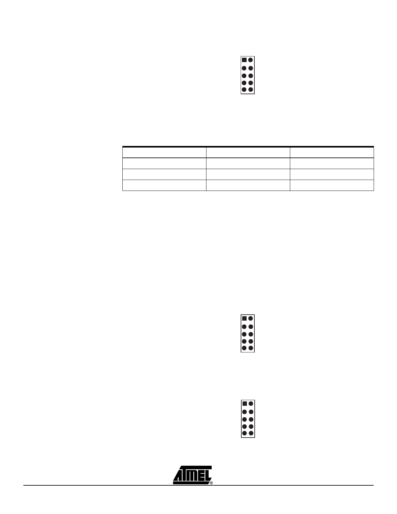
Figure 3-6. Pinout of PORTE Header
12
PE0
PE1
PE2
RST
REF
GND
XT1
XT2
GND
VTG
PORTE/AUX
The special functions of this port are:
n PE0 - PE2:
Table 3-1. PORTE Connection
ATmega161
PE0
PE0/ICP/INT2
PE1
PE1/ALE
PE2
PE2/OC1B
AT90S4414/AT90S8515
ICP
ALE
OC1B
n REF: Analog reference voltage. This pin is connected to the AREF pin on devices
having a separate analog reference pin.
n XT1: XTAL 1 pin. The internal main clock signal to all sockets. If the XTAL1 jumper is
disconnected, this pin can be used as external clock signal.
n XT2: XTAL 2 pin. If the XTAL1 jumper is disconnected, this pin can be used for
external crystal with the XT1 pin.
The headers for the LEDs and switches use the same pinout as the I/O port headers.
The pinout of the switch header is explained in Figure 3-7 and the pinout for the LED
header is explained in Figure 3-8. The square marking indicates pin 1.
Figure 3-7. Pinout of the Switch Header
12
SW0
SW1
SW2
SW3
SW4
SW5
SW6
SW7
GND
VTG
SWITCHES
Figure 3-8. Pinout of the LED Header
12
LED0
LED1
LED2
LED3
LED4
LED5
LED6
LED7
GND
VTG
LEDS
AVR STK500 User Guide
Share Link: 