GDC21D003 Ver la hoja de datos (PDF) - Hyundai Micro Electronics
Número de pieza
componentes Descripción
Fabricante
GDC21D003 Datasheet PDF : 77 Pages
| |||
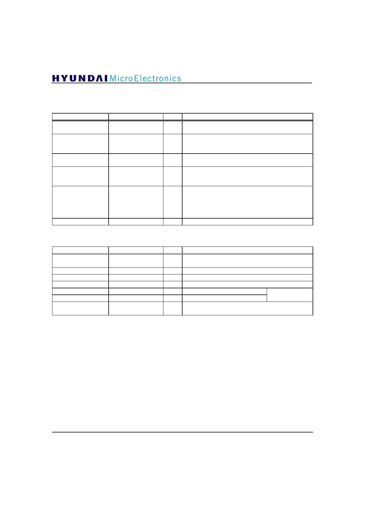
4.2 Pin Description
Clock/Reset ; 6 Pins
PIN
NAME
38
NRESET
12
VCXO
14
ADCCLK
18
CLKFS
37
CLK4FS
41
SYMCLK
A/D Converters ; 7 Pins
PIN
NAME
2
REF
121
COM
123
REFN
124
REFP
125
INN
126
INP
128
BIAS
GDC21D003
TYPE
I
I
O
O
I/O
I
DESCRIPTION
System reset(active low); This signal should be
activated on channel change or power on.
Clock input generated in VCXO; This pin can be
connected to one of two VCXOs whose output
frequencies are fs(10.76MHz) and 2fs(21.52MHz).
Clock for Off-chip ADC(21.52MHz or 10.76MHz);
This clock is generated by dividing VCXO input signal.
System clock; This clock is generated from dividing
VCXO input signal. Its frequency is the same of symbol
rate(10.76MHz).
Test clock/4x symbol clock;
When PLLEN(pin35) input is set to ‘1’, this pin is used
as 4x symbol clock output.
When PLLEN(pin35) input is set to ‘0’, this pin is used
as test clock(43.04MHz) input.
System clock input(10.76MHz)
TYPE
I
I
I
I
I
I
I
DESCRIPTION
Bias register for internal ADC; This pin should be
connected to AVDD(3.3V) via 12k ohm register.
Common voltage(1.5V)
Reference voltage(bottom: 1.2V)
Reference voltage(top: 2.2V)
Analog data input(negative)
Analog data input(positive)
1.65 ± 0.5V
differential
Bias input(2V typical) for On-chip ADC; This pin
should be connected to AVSS via 0.1µF capacitor.
12
Share Link: 