CA1523 Ver la hoja de datos (PDF) - Intersil
Número de pieza
componentes Descripción
Fabricante
CA1523 Datasheet PDF : 6 Pages
| |||
Specifications CA1523
Absolute Maximum Ratings
Thermal Information
DC Supply Voltage . . . . . . . . . . . . . . . . . . . . . . . . . . . . . . . . . . . 15V
Supply Current
|6(MAX). . . . . . . . . . . . . . . . . . . . . . . . . . . . . . . . . . . . . . . . . . . . . . ±50mA
|6(MAX), 1µs,1800pF Load . . . . . . . . . . . . . . . . . . . . +300, -200mA
Device Dissipation
Up to TA = 70oC . . . . . . . . . . . . . . . . . . . . . . . . . . . . . . . . 530mW
Above TA = 70oC . . . . . . . . . . . . . . Derate Linearly at 6.7mW/oC
Thermal Resistance
Plastic DIP Package . . . . . . . . . . . . . . . . . . . . . . . .
θJA
120oC/W
Device Dissipation
Up to TA = 70oC. . . . . . . . . . . . . . . . . . . . . . . . . . . . . . . . . 665mW
Ambient Temperature Range
Operating. . . . . . . . . . . . . . . . . . . . . . . . . . . . . . . . . 0oC to +70oC
Storage . . . . . . . . . . . . . . . . . . . . . . . . . . . . . . . . -55oC to +150oC
Lead Temperature (During Soldering)
At distance 1/16 ± in. (1.59mm ±0.79mm)
from case for 10s Max . . . . . . . . . . . . . . . . . . . . . . . . . . . . +265oC
CAUTION: Stresses above those listed in “Absolute Maximum Ratings” may cause permanent damage to the device. This is a stress only rating and operation
of the device at these or any other conditions above those indicated in the operational sections of this specification is not implied.
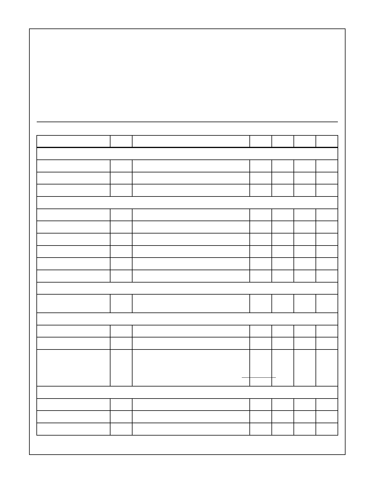
Electrical Specifications TA = +25oC, Refer to condition shown in test circuit; V7 = 13V, V1 = 5.9V Unless Otherwise Specified
PARAMETERS
PIN
TEST CONDITIONS
MIN
TYP MAX UNITS
POWER SUPPLY, VCC (PIN 7)
Supply Voltage
7
9.5
13
-
V
Supply Current
Zener Voltage
7
VCC = +13V
13
20
27
34
mA
7.8
8.4
8.9
V
OUTPUT PULSE (PIN 6)
Maximum Pulse Width
6
Measured at 6V Threshold Level
5.5
6.5
7.5
µs
Minimum Pulse Width
6
Measured at 6V Threshold Level
2
3
4
µs
Output High Voltage
Output Low Voltage
Rise Time
6
|6 = 0mA, V4 = 0V
6
|6 = 50mA, V12 = 0V
6
Measured at 1.8V and 10V Threshold Levels
11.1
12
12.6
V
0.6
1
1.3
V
250
600
1250
ns
Fall Time
6
Measured at 1.8V and 10V Threshold Levels
50
200
350
ns
ERROR VOLTAGE RANGE (PIN 1)
Error Voltage Reference
1
Adjust RT; Observe Pin 6 Min/Max
Frequency Range
5.9
6.8
7.5
V
CHARGE CURRENT (PIN 14)
Charge Current
Discharge Current
Slow Start Discharge Current
14 Adjust RT, V1 = 7.5V; Set V14 = 0V, Then V14 = 2.5V 190
220
250
µA
14 Adjust RT = 5.9V; Set V14 = 5.5V, Then 5V
95
110
125
µA
14 Maintain V14 = 5V, V10 = 5.5V
Set V10 = 5.5V, Measure I14 (Hi)
Set V10 = 4V, Measure I14 (Lo)
Limits = I14 (Hi) - I14 (Lo)
1.5
20
30
40
µA/V
LOGIC TESTS
Discharge Voltage
10 Pin 12 = 1kΩ to GND
1.7
2.4
3.2
V
Output Inhibit Voltage
Overcurrent Trip Voltage
7
Increase V7 Until V9 ≥ 2V
7.9
8.4
9.1
V
11
V12 = 5V; V10 = 0V; Increase V11 Until V9 ≤ 0.5V
1.1
1.25
1.4
V
2
Share Link: 