SL34118D Ver la hoja de datos (PDF) - System Logic Semiconductor
Número de pieza
componentes Descripción
Fabricante
SL34118D Datasheet PDF : 12 Pages
| |||
SL34118
the other (RLI2) is at the output of the speaker
amplifier. On the transmit side, one level detector
(TLI2) is at the output of the microphone amplifier,
while the other (TLI1) is at the hybrid output. Outputs
RLO1 and TLO1 feed a comparator, the output of
which goes to the Attenuator Control Block. Likewise,
outputs RLO2 and TLO2 feed a second comparator
which also goes to the Attenuator Control Block. The
truth table for the effects of the level detectors on the
Control Block is given in the section describing the
Control Block.
BACKGROUND NOISE MONITORS
The purpose of the background noise monitors is
to distinguish speech (which consists of bursts) from
background noise (a relatively constant signal level).
There are two background noise monitors - one for
the receive path and one for the transmit path.
Refering to Figure 2, the receive background noise
monitor is operated on by the RLI1-RLO1 level
detector, while the transmit background noise monitor
is operated on by the TLI2-TLO2 level detector. They
monitor the background noise by storing a dc voltage
representative of the respective noise levels in
capacitors at CPR and CPT. The voltages at these
pins have slow rise times (determined by the external
RC), but fast decay times. If the signal at RLI1 (or
TLI2) changes slowly, the voltage at CPR (or CPT)
will remain more positive than the voltage at the non-
inverting input of the monitor’s output comparator.
When speech is present, the voltage on the
noninverting input of the comparator will rise quicker
than the voltage at the inverting input (due to the
burst characteristic of speech), causing its output to
change. This output is sensed by the Attenuator
Control Block.
The 36 mV offset at the comparator’s input keeps
the comparator from changing state unless the
speech level exceeds the background noise by
≈4.0 dB. The time constant of the external RC
(≈4.7 seconds) determines the response time to
background noise variations
VOLUME CONTROL
The volume control input at VLC (Pin 13) is
sensed as a voltage with respect to VB. The volume
control affects the attenuators only in the receive
mode. It has no effect in the idle or transmit modes.
When in the receive mode, the gain of the receive
attenuator will be +6.0 dB, and the gain of the transmit
attenuator will be -46 dB only when VLC is equal to
VB. As VLC is reduced below VB,
the gain of the receive attenuator is reduced, and the
gain of the transmit attenuator is increased such that
their sum remains constant. Changing the voltage at
VLC changes the voltage at CT (see the Attenuator
Control Block section), which in turn controls the
attenuators.
The volume control setting does not affect the
maximum attenuator input signal at which notice able
distortion occurs.
The bias current at VLC is typically 60 nA out of
the pin, and does not vary significantly with the VLC
voltage or with VCC.
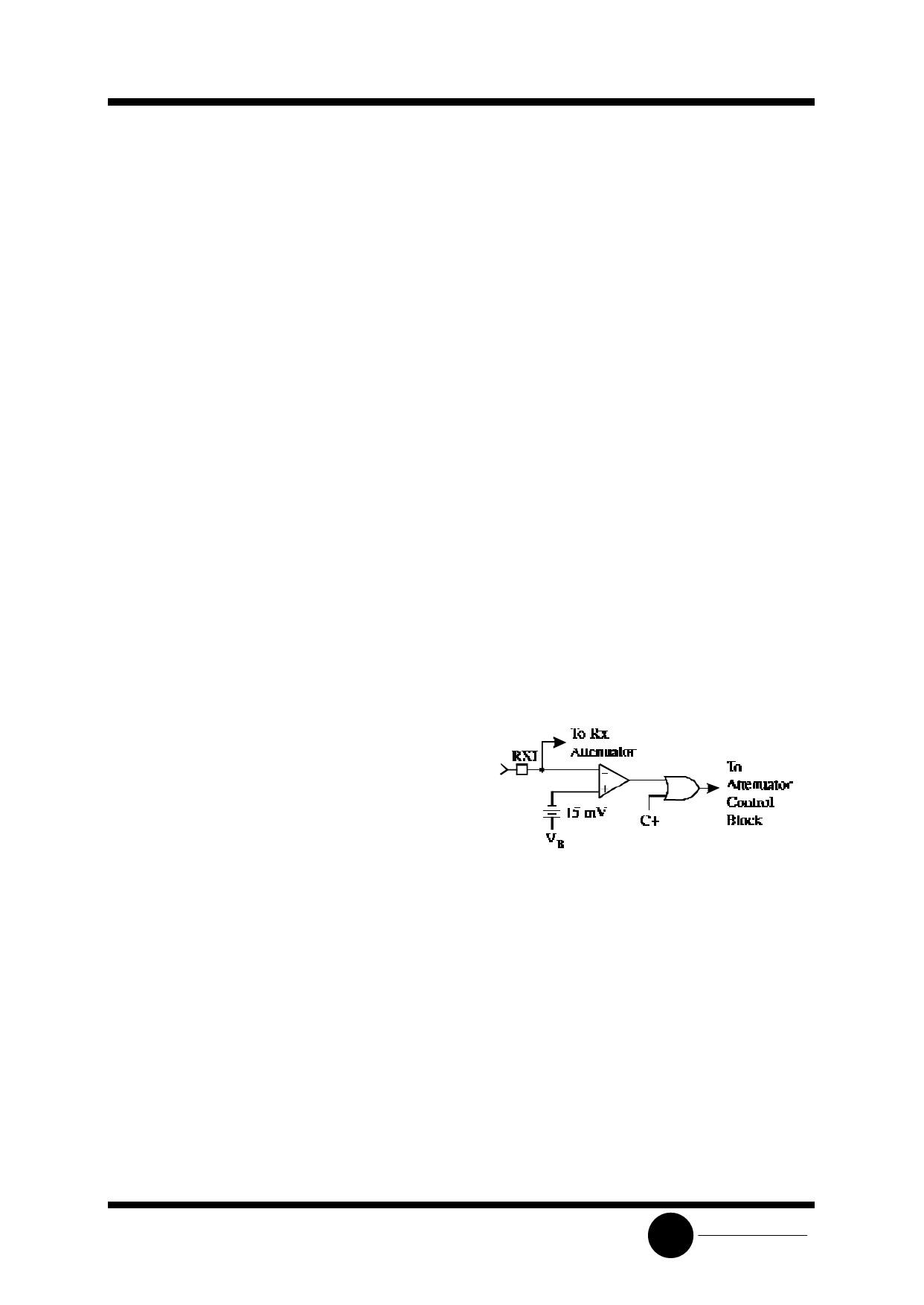
DIAL TONE DETECTOR
The dial tone detector is a comparator with one
side connected to the receive input (RXI) and the
other input connected to VB with a 15 mV offset (see
Figure 3). If the circuit is in the receive mode, and the
incoming signal is greater than 15 mV (10 mVrms), the
comparator’s output will change, disabling the
receive idle mode. Tthe receive attenuator will then be
at a setting determined solely by the volume control.
The purpose of this circuit is to prevent the dial
tone (which would be considered as continuous
noise) from fading away as the circuit would have the
tendency to swich to the idle mode. By disabling the
receive idle mode, the dial tone remains at the
normally expected full level.
Figure 3. Dial Tone Detector
AGS
The AGS circuit affects the circuit only in the
receive mode, and only when the supply voltage (VCC)
is less than 3.5 volts. As VCC falls below 3.5 volts, the
gain of the receive attenuator is reduced. The transmit
path attenuation changes such that the sum of the
transmit and receive gains remains constant.
The purpose of this feature is to reduce the power
(and current) used by the speaker when a line-
powered speakerphone is connected to a long line,
where the available power is limited. By reducing the
speaker power, the voltage sag at VCC is controlled,
preventing possible erratic operation.
SLS
System Logic
Semiconductor
Share Link: 