BH3810FS Ver la hoja de datos (PDF) - ROHM Semiconductor
Número de pieza
componentes Descripción
Fabricante
BH3810FS Datasheet PDF : 9 Pages
| |||
Multimedia ICs
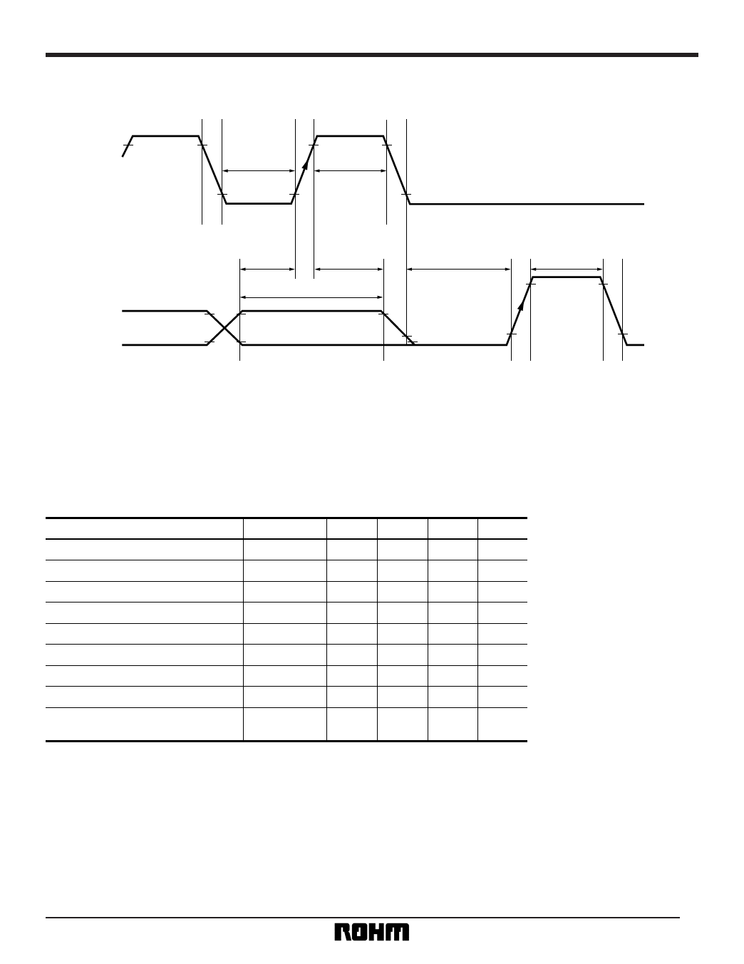
(2) Timing chart
Serial data timing (timing for the IC terminals)
SCK
(clock signal)
90%
tw
tw
10%
BH3810FS
SI
(DATA signal,
D22
LATCH signal)
tsu
th
tw (DATA)
90%
D23
10%
ts
tw (LATCH)
90%
10%
∗ When LATCH is "H", the DATA signal is forced "L" internally.
∗ The read decision for the DATA signal (SI) is made by the signal when the CLOCK signal rises.
∗ The read decision for the LATCH signal (SI) is made by the signal when the LATCH signal itself rises.
∗ A "L" must follow at the end of each signal to wait for the next signal.
Fig.3
•Timing chart constants (Ta = 25°C, VDD = 5V and VEE = – 4V)
Parameter
Symbol
Min. Typ. Max. Unit
H input voltage
VIH
4.0
5.0
6.0
V
M input voltage
VIM
2.0
2.5
3.0
V
L input voltage
VIL
– 0.3
0
1.0
V
Minimum clock width
tw
2.0
—
—
µs
Minimum data width
tw (DATA) 4.0
—
—
µs
Minimum latch width
tw (LATCH) 2.0
—
—
µs
Setup time (DATA to CLK)
tsu
1.0
—
—
µs
Hold time (CLK to DATA)
th
1.0
—
—
µs
Setup time (DATA, CLK to LATCH)
ts
1.0
—
—
µs
∗ If the voltage between VDD and DGND changes, the values above will change.
7
Share Link: 