GS4882 Ver la hoja de datos (PDF) - Gennum -> Semtech
Número de pieza
componentes Descripción
Fabricante
GS4882 Datasheet PDF : 7 Pages
| |||
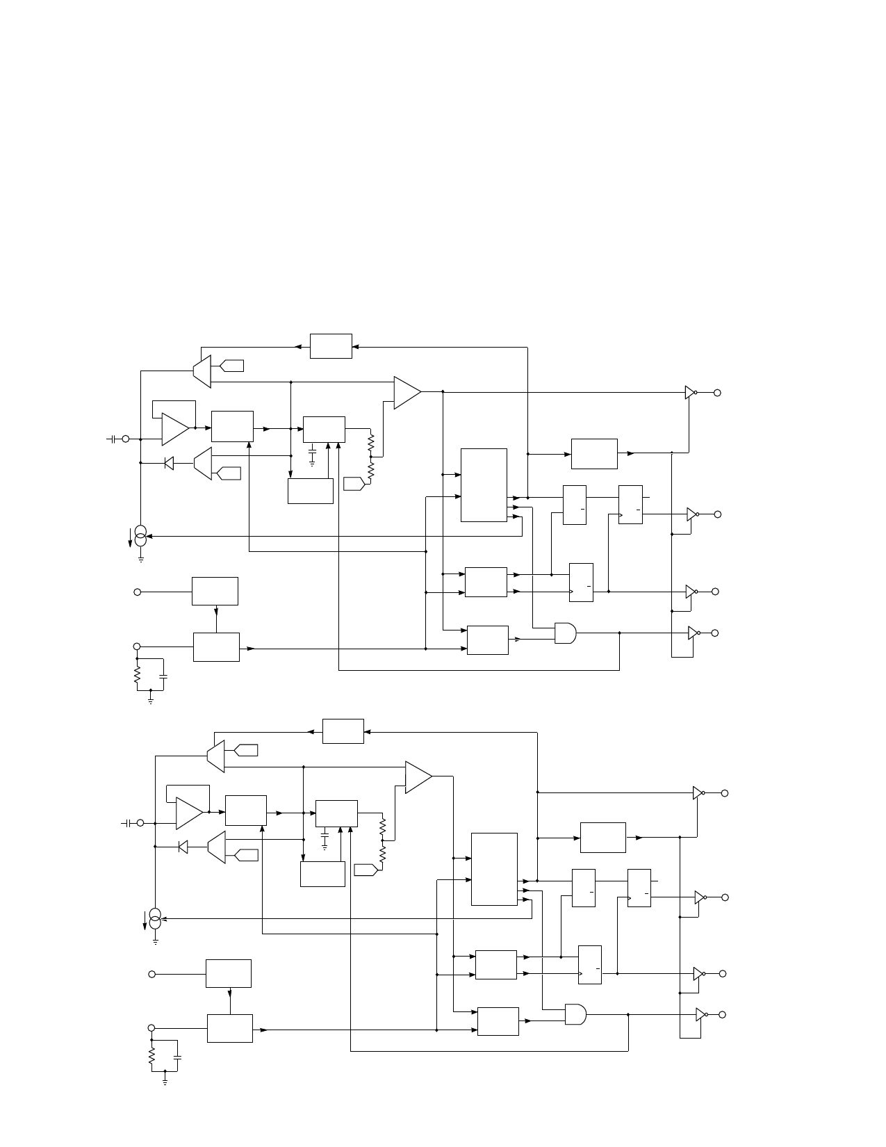
SIGNAL DETECT AND OUTPUT MUTE
Internal to the GS4882 and GS4982 is a robust video signal
detection circuit. This circuit provides a reliable control signal
that will enable the sync separator outputs only when a valid
video signal is present. When the input signal is not valid, the
outputs are muted and stay in a logic high state.
The GS4882 and GS4982 differentiate between valid and in-
valid input signals by feeding the horizontal sync information
into a frequency to voltage converter. The horizontal scan rate
of the input signal is then compared to an expected input
signal horizontal scan rate. With RSET=227 kΩ, the sync
separator will typically define a valid input signal as one with
a horizontal frequency of 15.7 ± 4 kHz.
Assuming that the sync separator is in steady state operation
with a valid input signal, all outputs will be enabled. Removal
of the input signal, or a significant change in the input signal
frequency, will cause an internal probation timer to be triggered.
While on probation, the sync separator outputs remain
enabled and separated sync is still produced. If a valid input
signal is not returned to the system before the probation time
expires (typically 2.5 ms), all outputs will be muted to logic
high state. Should a valid signal return during the probation
period, and eight lines be received before the probation time
expires, device outputs will remain enabled. Once device
outputs are muted, the device must receive 8 valid lines of
video at the correct horizontal frequency before the outputs
are re-enabled.
CLEN
+
VSC
-
CCLLAAMMPP
WWIINNDDOOWW
HORIZONTAL
-
COMPOSITE
SYNC OUTPUT
(Pin 1)
+
VIDEO
INPUT
-
(Pin 2)
+
0.1µ
2NDFIOLTREDRER
BBEESSSSEELL
2NFDILOTREDRER
-
+ VHC
IINNTTEEGGRRAATTEEDD
HHOOLLDD
R
50%
POINT
R
FFAAUULLTT
VSC
HHAANNDDLLIINNGG
WINDOWING
CIRCUIT
SIGNAL
DETECT
MUTE
DQ
GQ
DQ
CLK Q
ODD / EVEN
OUTPUT
(Pin 7)
NO SYNC
VCC
(Pin 8)
RSET
(Pin 6)
227k
VOLTAGE
REGULATOR
TIMING
CURRENTS
0.1µ
VERTICAL
DETECTOR
BACK PORCH
DETECTOR
DQ
CLK Q
BPEN
Fig. 6 GS4882 Block Diagram
VERTICAL SYNC
OUTPUT
(PIN 3)
BACK PORCH
OUTPUT
(Pin 5)
VIDEO
INPUT
-
(Pin 2)
+
0.1µ
CLEN
+
VSC
-
2ND ORDER
BESSEL
FILTER
-
+
VHC
NO SYNC
CLAMP
WINDOW
HORIZONTAL
-
+
INTEGRATED
HOLD
R
50%
POINT
R
FAULT
VSC
HANDLING
WINDOWING
CIRCUIT
HORIZONTAL
(Pin 1)
SIGNAL
DETECT
MUTE
DQ
GQ
DQ
CLK Q
ODD / EVEN
OUTPUT
(Pin 7)
VCC
(Pin 8)
RSET
(Pin 6)
227k
VOLTAGE
REGULATOR
TIMING
CURRENTS
0.1µ
VERTICAL
DETECTOR
BACK PORCH
DETECTOR
DQ
CLK Q
BPEN
Fig. 7 GS4982 Block Diagram
5 of 7
VERTICAL SYNC
OUTPUT
(PIN 3)
BACK PORCH
OUTPUT
(Pin 5)
521 - 61 - 01
Share Link: 