GS4882 Ver la hoja de datos (PDF) - Gennum -> Semtech
Número de pieza
componentes Descripción
Fabricante
GS4882 Datasheet PDF : 7 Pages
| |||
CIRCUIT DESCRIPTION
COMPOSITE SYNC OUTPUT (pin 1 GS4882)
The Block Diagrams for the GS4882 and GS4982 are shown
in Figure 6 and Figure 7, with timing diagrams for the devices
shown in Figure 8.
The filtered video signal is then fed to a comparator which
compares it to an internally derived voltage corresponding to
the 50% point of the sync pulse amplitude.
When presented with a composite video input signal, the
GS4882 outputs composite sync, vertical sync, back porch
and odd/even field information. The GS4982 substitutes the
composite sync output with a horizontal sync output, for those
applications requiring horizontal sync extraction.
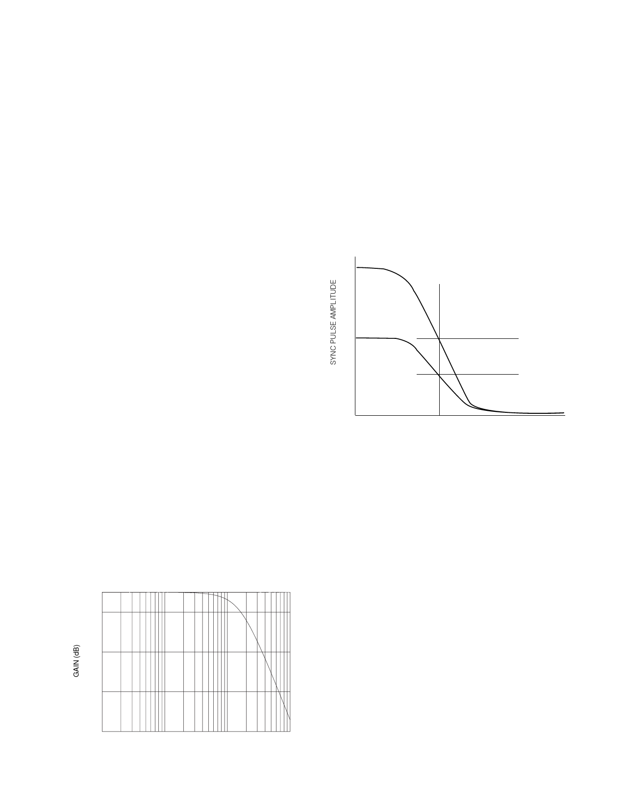
By slicing the composite video waveform at 50% of the sync
pulse amplitude, variations in output pulse timing due to
variations in input signal amplitude are minimized. Figure 1
demonstrates the stability of output pulse timing achieved with
50% sync slicing .
An external resistor, RSET, connected to pin 6 is used to set all
timing currents in the device. For standard NTSC applications,
RSET should be set to 227 kΩ. The value of RSET for a standard
NTSC application is different for the GS4882/GS4982 line of
sync separators(RSET = 227 kΩ) than it is for the GS1881/
GS4881/GS4981 line of sync separators (RSET = 680 kΩ). This
change was made to improve jitter performance of the device.
With 50% Sync Slicing no Time Base Errors (TBEs)
are introduced due to variations in sync pulse amplitude.
Output pulses are always produced at tO+tD , where
tD represents the delay through the device.
A Sync Pulse No.1
COMPOSITE VIDEO INPUT (pin 2)
The GS4882 and GS4982 will operate with input signal
amplitudes ranging from 0.5 V to 4.0 V p-p. Composite video
is AC coupled into the device via an external coupling
capacitor connected to pin 2.
A/2 Sync Pulse No.2
50% Slice
Immediately upon entering the GS4882/GS4982 the video
signal is passed to the device’s dual mode input clamp in
order to clamp the sync tip of the input video waveform to 1.55
Volts. The GS4882/GS4982’s dual mode input clamp, with
both Hard Clamp and Soft Clamp capabilities, has been
specifically designed for use in high performance sync sepa-
ration. The dual mode input clamp aids in maintaining the
accuracy of the internally derived 50% sync slicing level to
within ±5% by utilizing the Soft Clamp during steady state
operation. The device improves system start-up and impulse
noise recovery time by utilizing the device’s Hard Clamp and
Nosync Recovery Current during initial start-up and when
steady state operation has been disturbed by impulse noise.
During the clamping operation, the input video signal is
passed through the device's internal color burst filter. The
internal filter attenuates the color burst by typically >15 dB.
Figure 1 shows the typical frequency response of the internal
color burst filter.
0
-5
-15
50% Slice
to
Time
Fig. 2 Stability of Output Pulse Timing with Variations
in Sync Pulse Amplitude
The 50% point of sync is determined by using two identical
resistors to divide the voltage between sync tip and back
porch. The importance of precision sync tip clamping may be
appreciated here, since the sync tip voltage is used in deriving
the 50% slicing level. The back porch voltage is derived
through an internal integrate and hold circuit that is gated by
the Back Porch output signal. By integrating over the entire
back porch period, the accuracy and noise immunity of
acquired back porch voltage is greatly improved when
compared to systems using simple sample and hold
techniques.
The output of the comparator is a reproduction of the input
video signal with the active portion of video removed. This
represents the composite sync waveform presented on pin 1
of the GS4882.
The video path and composite sync slicing circuitry have been
-25
optimized and compensated to achieve superior temperature
stability. Variations in composite sync output timing over the
commercial temperature range are less than ±5 ns.
-35
0.01
0.1
1
10
FREQUENCY (MHz)
Fig. 1 Frequency Response of Internal Color Burst Filter
3 of 7
521 - 61 - 01
Share Link: 