LA7415 Ver la hoja de datos (PDF) - SANYO -> Panasonic
Número de pieza
componentes Descripción
Fabricante
LA7415 Datasheet PDF : 12 Pages
| |||
LA7415
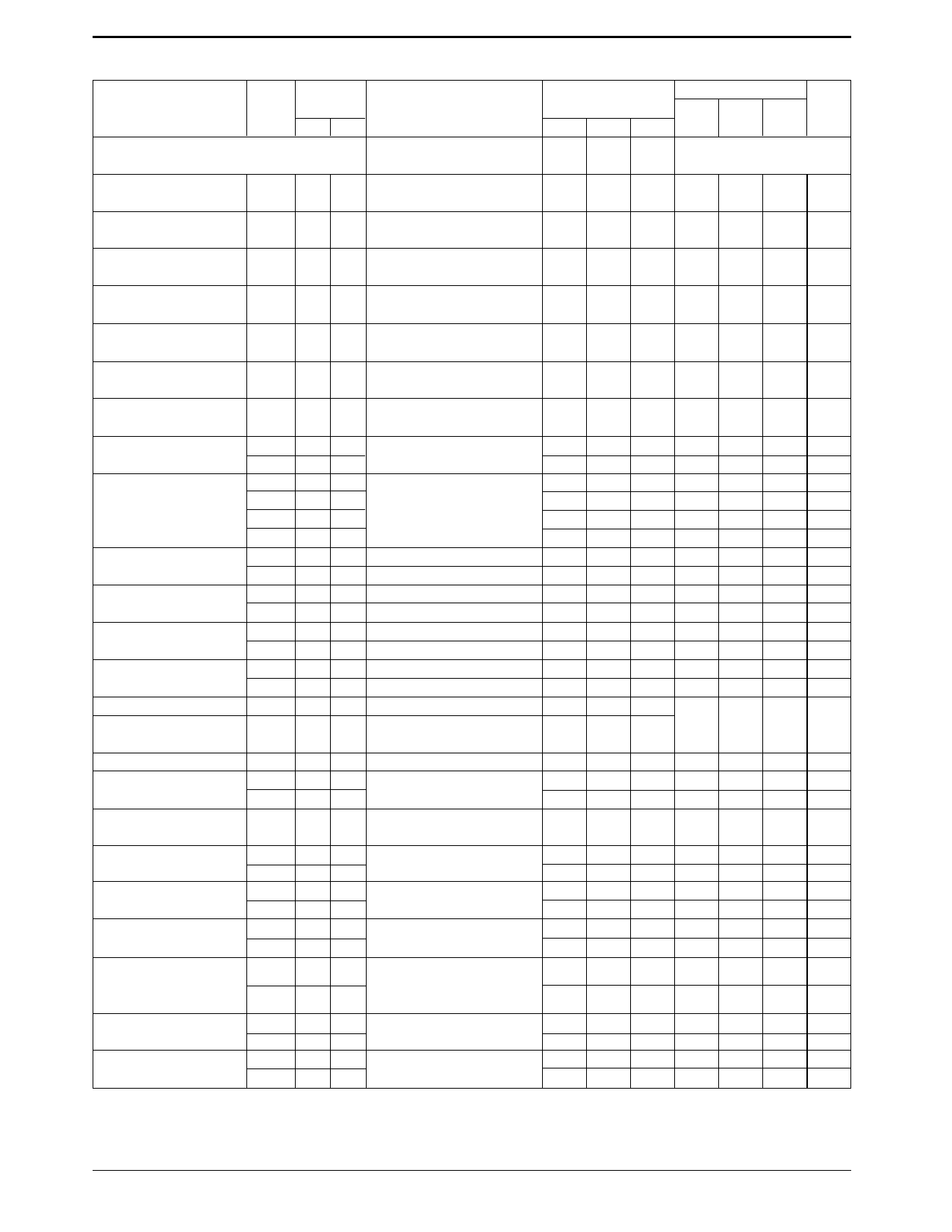
Continued from the preceding page.
Parameter
Symbol
Input Output
Conditions
T15: 5.0 V, T13: OPEN,
T7: OPEN
Ratings
Unit
min typ max
T2
T4
T5
TRCK
HA SW30
MUTE
Enveloped detector
output pin voltage
VENV
T8 The T8 DC voltage with no input OPEN 0
0
0
0.4
0.8 V
Enveloped detector
voltage SP1
VENVSP1 T20A T8
f = 4 MHz
T10A: Adjusted to 300 mV p-p
OPEN
0
0
2.1
2.6
3.1 V
Enveloped detector
voltage SP2
VENVSP2 T20A T8
f = 4 MHz
T10A: Adjusted to 600 mV p-p
OPEN
0
0
4.5
4.8
5.0 V
Enveloped detector
voltage EP1
VENVEP1 T27A T8
f = 4 MHz
T10A: Adjusted to 200 mV p-p
OPEN 5.0
0
2.0
2.6
3.0 V
Enveloped detector
voltage EP2
VENVEP2 T27A T8
f = 4 MHz
T10A: Adjusted to 450 mV p-p
OPEN 5.0
0
4.5
4.8
5.0 V
Comparator
output voltage 1
VCOMP1 T20A T3
f = 4 MHz, VIN = 38 mVp-p
The T3 DC voltage
5.0
0
0
–
0.4
0.7 V
Comparator
output voltage 2
VCOMP2 T20A T3
f = 4 MHz, VIN = 38 mVp-p
The T3 DC voltage
5.0
Playback mode on switching
transistor on resistance
Playback mode
mode switching
transistor on
resistance
Trick 1 threshold
level
Trick 2 threshold
level
HAPB threshold
level
SW30 threshold
level
RPON17
RPON18
RPON21
RPON24
RPON26
RPON29
TR1-1
TR1-2
TR2-1
TR2-2
HAP-1
HAP-2
SW30-1
SW30-2
P-17
P-18
P-21
P-24
P-26
P-29
T2
T2
T2
T2
T4
T4
T5
T4
The difference in the DC measurement
for 1-mA and 2-mA influx currents
The difference in the DC measurement
for 1-mA and 2-mA influx currents
Normal → Trick1
Trick1 → Normal
Normal → Trick2
Trick2 → Normal
SP → EP
EP → SP
Lch → Hch
Hch → Lch
–
–
OPEN
OPEN
OPEN
OPEN
*
*
*
*
–
–
–
–
T2
[Record Mode]
T15: 5.0 V, T2: OPEN,
T6: 5.0 V, T7: 5.0 V
REC
Adj2
Current drain
AGC amplifier
output level
Inter-mode gain
difference
ICCR
VRSP
VREP
T11A T21A
T11A T26A
The pin 15 influx current
f = 4 MHz
VIN = 200 mVp-p
∆VGR
–
– VRSP/VREP
OPEN
OPEN
OPEN
–
AGC amplifier control
characteristics 1
AGC amplifier control
characteristics 2
AGC amplifier frequency
characteristics
AGC amplifier second
harmonic distortion
∆VAGC1-SP T11A T21A
∆VAGC1-EP T11A T26A
∆VAGC2-SP T11A T21A
∆VAGC2-EP T11A T26A
∆VFRS T11A T21A
∆VFRE T11A T26A
f = 4 MHz, VIN = 400 mVp-p
The output level/VRSP, EP ratio
f = 4 MHz, VIN = 100 mVp-p
The output level/VRSP, EP ratio
f = 1 MHz, 7 MHz, VIN = 100 mVp-p
The 7 MHz/1 MHz output ratio
OPEN
OPEN
OPEN
OPEN
OPEN
OPEN
∆VHDRS
∆VHDRE
T11A T21A
T11A T21A
f = 4 MHz, VIN = 200 mVp-p
The (8 MHz component)/(4 MHz component)
output ratio
OPEN
OPEN
AGC amplifier maximum
output level
AGC amplifier muting
attenuation
∆VOMRS
∆VOMRE
∆VMRS
∆VMRE
T11A T21A
T11A T26A
T11A T21A
T11A T26A
f = 4 MHz, The output level for which
the second harmonic is –35 dB
f = 4 MHz, VI = 200 mVp-p
The output level/VRSP, EP ratio
Adj.
Adj.
OPEN
OPEN
5.0
0
–
–
–
–
5.0
–
5.0
–
0
–
0
–
–
–
–
–
–
–
–
–
*
–
*
–
–
*
–
*
T4
T5
HA SW30
MUTE
0
0
0
0
5.0
0
–
–
0
0
5.0
0
0
0
5.0
0
0
0
5.0
0
0
0
5.0
0
0
0
5.0
0
0
5.0
5.0
5.0
4.5
4.8
–V
–
4.0
6.0 Ω
–
4.0
6.0 Ω
–
4.0
6.0 Ω
–
4.0
6.0 Ω
–
4.0
6.0 Ω
–
4.0
6.0 Ω
3.2
–
5.0 V
1.2
–
2.8 V
0.0
–
0.8 V
1.2
–
2.8 V
1.8
–
5.0 V
0.0
–
1.4 V
1.2
–
5.0 V
0.0
–
0.8 V
44
55
66 mA
147 156 165 mVp-p
116 123 130 mVp-p
1.30 2.05 2.80 dB
–
0.5
1.0 dB
–
0.5
1.0 dB
–1.0 –0.5
– dB
–1.0 –0.5
– dB
–1.0 –0.0 +1.0 dB
–1.0 –0.0 +1.0 dB
– –45 –40 dB
– –45 –40 dB
20
22
– mAp-p
20
22
– mAp-p
– –45 –40 dB
– –45 –40 dB
Continued on the next page.
No. 5647-3/12
Share Link: 