CMX624 Ver la hoja de datos (PDF) - CML Microsystems Plc
Número de pieza
componentes Descripción
Fabricante
CMX624 Datasheet PDF : 26 Pages
| |||
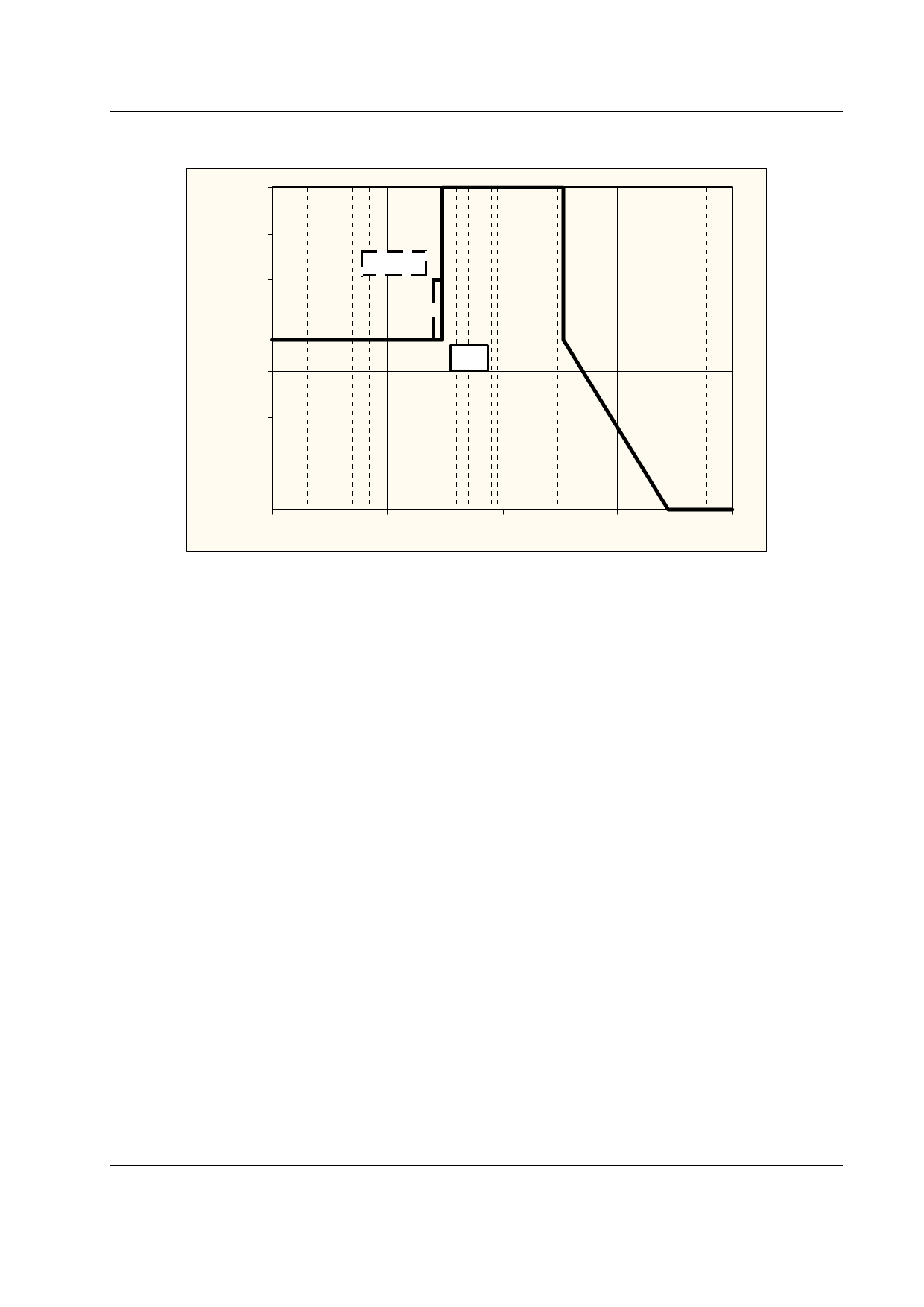
V23 / Bell 202 Modem
CMX624
0
-10
Bell 202
-20
-30
dBm
V23
-40
-50
-60
-70
10
100
1000 Hz 10000
100000
Figure 5 Maximum Out of Band Tx Line Energy Limits
1.5.8 Transmit Output Buffer
This buffer amplifier, connected to the TXN, TXO and TXON pins, is intended for use as a Tx line driver as
shown in Section 1.6.1. Two symmetrical outputs are provided for use with a balanced load to give
sufficient Tx line signal levels even at low VDD. If this is not required the TXON output can be disabled.
If the buffer is used as a balanced line driver, then bit 6 of the SETUP Register should be set to ‘1’ (TXON
output enabled). Setting bit 6 to ‘0’ disables the TXON output and the buffer draws less current from the
supply. When bit 6 is set to '0' the TXON pin should be left open circuit. N.B. The TXO output is unaffected
by this bit.
1.5.9 Ring Signal Detector
This block, which functions even in Zero Power mode, can be used to detect a telephone line Ring Signal
or Line Voltage Reversal and then generate a Interrupt Request signal to wake up the µC at the start of a
call. Suitable interface circuits are shown in Section 1.6.2.
The output of this block is the ‘Ring Detect’ line shown in Figure 1 which directly drives bit 6 of the FLAGS
Register. Any ‘0’ to ‘1’ or ‘1’ to ‘0’ change on this line will also set the ‘Ring Detect Change’ bit (5) of the
FLAGS Register.
If this block is not used, then the RD and RT pins should be connected to VSS and the ‘Ring Detect
Change’ bit (5) of the IRQ MASK Register set to ‘0’.
2003 CML Microsystems Plc
10
D/624/7
Share Link: 