ST3L01 Ver la hoja de datos (PDF) - STMicroelectronics
Número de pieza
componentes Descripción
Fabricante
ST3L01 Datasheet PDF : 12 Pages
| |||
ST3L01
ABSOLUTE MAXIMUM RATINGS
Symbol
VCC
VDD
VESD
Tstg
TJ
Parameter
Supply Voltage
ISupply Voltage
ESD Tolerance (Human Body Model)
Storage Temperature Range
Operating Junction Temperature Range
GENERAL OPERATING CONDITION
Symbol
VCC
∆VCC
tr
tf
VDD
∆VDD
tr
tf
TAl
Parameter
VCC Supply Voltage
VCC Ripple
Rise Time (10% to 90%) referred to VCC
Fall Time (90% to 10%) referred to VCC
VDD Supply Voltage
VDD Ripple
Rise Time (10% to 90%) referred to VDD
Fall Time (90% to 10%) referred to VDD
Operating Ambient Temperature Range
THERMAL DATA
Symbol
Parameter
Rthj-case Thermal Resistance Junction-case
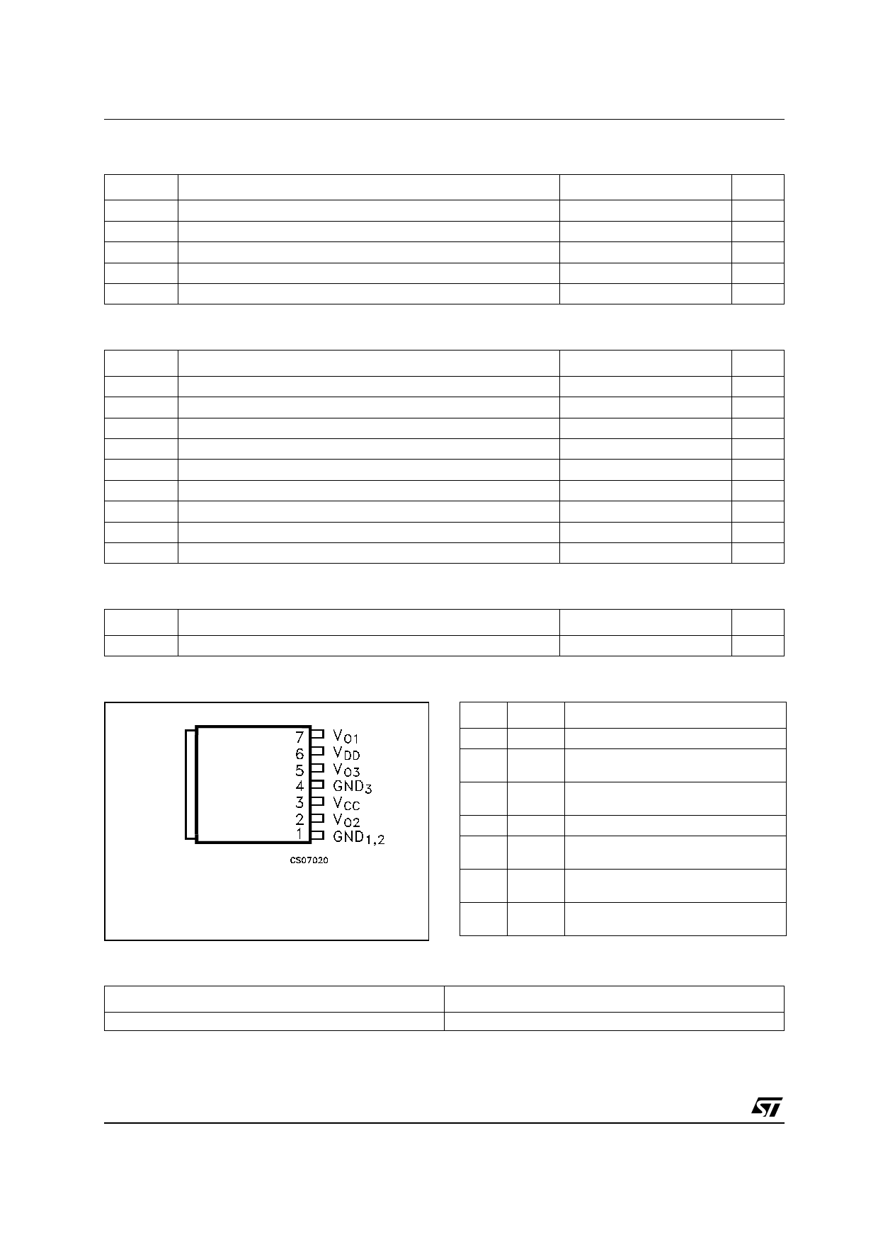
CONNECTION DIAGRAM (top view)
SPAK-7L
ORDERING INFORMATION
TYPE
ST3L01
(*) Available in Tape & Reel with the suffix "R"
Value
Unit
18
V
18
V
4
KV
-65 to +150
°C
0 to +150
°C
Value
Unit
4.75 to 5.25
V
±0.15
V
1
V
1
V
10.8 to 13.2
V
±0.3
V
1
V
1
V
0 to 70
µs
SPAK-7L
2
Unit
°C/W
PIN DESCRIPTION
Pin N° Symbol
Name and Function
1 GND1,2 VO1 and VO2 regulators GND pin
2
VO2 Second Output Pin: Bypass with a
0.1µF capacitor to GND
3
VCC Input Pin: Bypass with a 0.1µF
capacitor to GND
4
GND3 VO3 regulators GND pin
5
VO3 Third Output Pin: Bypass with a
0.1µF capacitor to GND
6
VDD Input Pin: Bypass with a 0.1µF
capacitor to GND
7
VO1 First Output Pin: Bypass with a 0.1µF
capacitor to GND
SPAK (Power Flex™) 7 leads (*)
ST3L01K7
2/12
Share Link: 