CXD2498 Ver la hoja de datos (PDF) - Sony Semiconductor
Número de pieza
componentes Descripción
Fabricante
CXD2498 Datasheet PDF : 51 Pages
| |||
CXD2498R
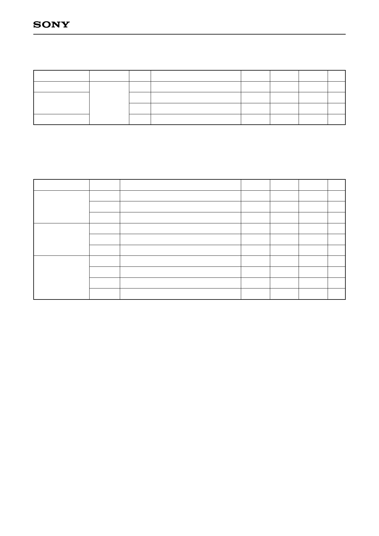
Inverter Input Characteristics for Base Oscillation Clock Duty Adjustment
(Within the recommended operating conditions)
Item
Pins
Logical Vth
Input voltage
CKI
Input amplitude
Symbol
Conditions
LVth
VIH
VIL
VIN fmax = 50MHz sine wave
Min.
0.7VDDc
0.3
Typ.
VDDc/2
Max. Unit
V
V
0.3VDDc V
Vp-p
Note) Input voltage is the input voltage characteristics for direct input from an external source.
Input amplitude is the input amplitude characteristics in the case of input through a capacitor.
Switching Characteristics
(VH = 15.0V, VM = GND, VL = –7.5V)
Item
Rise time
Fall time
Output noise
voltage
Symbol
TTLM
TTMH
TTLH
TTML
TTHM
TTHL
VCLH
VCLL
VCMH
VCML
VL to VM
VM to VH
VL to VH
VM to VL
VH to VM
VH to VL
Conditions
Min.
Typ.
Max. Unit
200
350
500 ns
200
350
500 ns
30
60
90 ns
200
350
500 ns
200
350
500 ns
30
60
90 ns
1.0
V
1.0
V
1.0
V
1.0
V
Note)
1) The MOS structure of this IC has a low tolerance for static electricity, so full care should be given for
measures to prevent electrostatic discharge.
2) For noise and latch-up countermeasures, be sure to connect a by-pass capacitor (0.1µF or more)
between each power supply pin (VH, VL) and GND.
3) To protect the CCD image sensor, clamp the SUB pin output at VH before input to the CCD image
sensor.
–7–
Share Link: 