NT3965 Ver la hoja de datos (PDF) - Novatek Microelectronics
Número de pieza
componentes Descripción
Fabricante
NT3965 Datasheet PDF : 12 Pages
| |||
NT3965
TFT LCD Source Driver
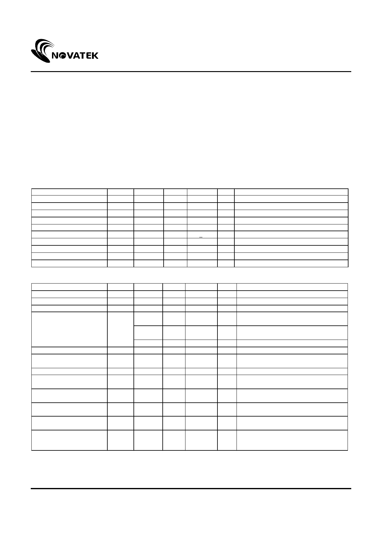
Absolute Maximum Ratings*
*Comments
Digital supply voltage, Vcc
-0.5V to 5V
Analog supply voltage, AVDD
-0.5V to +12V
Supply voltage, V1~ V5
0.4AVDD ~AVDD+0.3
Supply voltage, V6 ~ V10
-0.3 ~ 0.6AVDD
Digital input voltage
-0.5V to Vcc+0.5V
Output voltage, DIO1 & DIO2 -0.5V to Vcc+0.5V
Output voltage,OUT1~OUT384 -0.5V to AVDD+0.5V
Storage temperature
-55OCto 125OC
Operating temperature
-10OC to 75OC
Stresses above those listed under "Absolute Maximum
Ratings" may cause permanent damage to the device.
These are stress ratings only. Functional operation of this
device at these or under any other conditions above those
indicated in the operational sections of this specification are
not implied and exposure to absolute maximum rating
conditions for extended periods may affect device reliability.
DC Electrical Characteristics (Vcc =2.7~3.6V , AVDD=10V, AVSS=GND=0V, TA=-10OC~75OC)
(For the digital circuit)
Parameter
Symbol Min.
Typ. Max. Unit
Conditions
Supply Voltage
Vcc
2.7
3.3
3.6
V Digital power
Low Level Input Voltage
Vil
0
-
0.3xVcc V For the digital circuit
High Level Input Voltage
Vih 0.7xVcc
-
Vcc
V For the digital circuit
High Level Output Voltage
Low Level Output Voltage
Voh Vcc-0.4
Vol
GND
-
-
V DIO1, DIO2, Ioh=1mA
- GND+0.4 V DIO1, DIO2, Iol=-1mA
Input Leakage Current
Ii
-
-
+1
A For the digital circuit
Digital Stand-by Current
Ist
-
10
50
A All operating is stopped
Digital Operating Current
Icc
-
1.5
3
mA Fclk=45 MHz, FLD=50KHz
Input Loading 1
Input Loading 2
Ci1
-
Ci2
-
-
6
pF DIO1/2, V1~V10 exclusive
-
10
pF DIO1/2
(For the analog circuit)
Parameter
Symbol
Supply Voltage
AVDD
Input level of V1 ~ V5
Vref
Input level of V6 ~ V10
Vref
Min.
6.5
0.4AVDD
0.1
Voltage Output Swing
Deviation between Pins
-30
Vdp
-25
-10
Output Voltage deviation
Vod
-20
Voltage Output Offset
between Chips
Voc
-10
Dynamic Range of Output
Vdr
0.1
Sinking Current of Outputs IOL
-
Driving Current of Outputs
Impedance of Gamma
Correction
Analog Stand-by Current
IOH
150
Ri
0.8*Rn
Isc
-
Analog Operating Current
Ioc
-
Typ.
8.4
-
-
±20
Max.
10
AVDD-0.1
0.6AVDD
+30
±10
±7
-
-
-
-180
+25
+10
+20
+10
AVDD-0.1
-150
200
-
Rn 1.4*Rn
4
5.5
7
10
Unit
V
V
V
mV
mV
mV
mV
mV
V
A
A
ohm
mA
mA
Conditions
For the analog circuit power
Gamma correction voltage
Gamma correction voltage
Vo=0.1V ~ 0.8V & AVDD-0.8 ~ AVDD-
0.1V
Vo=0.8V ~ 1.2V & AVDD-1.2 ~ AVDD-
0.8V
Vo=1.2V ~ AVDD-1.2V
OUT1 ~ OUT384
OUT1 ~ OUT384; Vo=0.1V V.S 1.0V
AVDD=10V
OUT1 ~ OUT384; Vo=9.9V V.S 9V
AVDD=10V
Rn=15850 ohm, from V1~V5 & V6~V10
No load, Fclk=33MHz, FLD=50KHz
AVDD=8.4V, OUT=4.2V
No load, Fclk=33MHz, FLD=50KHz
AVDD=8.4V,V1=8V, V10=0.2V, Black-
white line
8
Version 2.0
Share Link: 