NT3965 Ver la hoja de datos (PDF) - Novatek Microelectronics
Número de pieza
componentes Descripción
Fabricante
NT3965 Datasheet PDF : 12 Pages
| |||
NT3965
TFT LCD Source Driver
Power on/off sequence:
This IC is a high-voltage LCD driver, so it may be damaged by a large current flow when an incorrect power sequence is
used. The recommended sequence should be: digital power (Vcc&GND)è logic signals èanalog power (AVDD&AVSS)
èGamma correction reference voltage(V1~V10). Reverse this sequence to shut down, or turn off all signals and power
simultaneously.
Relationship between the order of input data and output channels
(1) SHL=”1”, Start pulse from DIO1, shift right
Output OUT1 OUT2 OUT3 OUT4 OUT5 OUT6
---
Order
First data
--à
Data D05~D00 D15~D10 D25~D20 D35~D30 D45~D40 D55~D50 - - -
OUT384
Last data
D55~D50
(2) SHL=”0”, Start pulse from DIO2, shift left
Output OUT379 OUT380 OUT381 OUT382 OUT383 OUT384 - - -
Order
First data
--à
Data D05~D00 D15~D10 D25~D20 D35~D30 D45~D40 D55~D50 - - -
OUT6
Last data
D55~D50
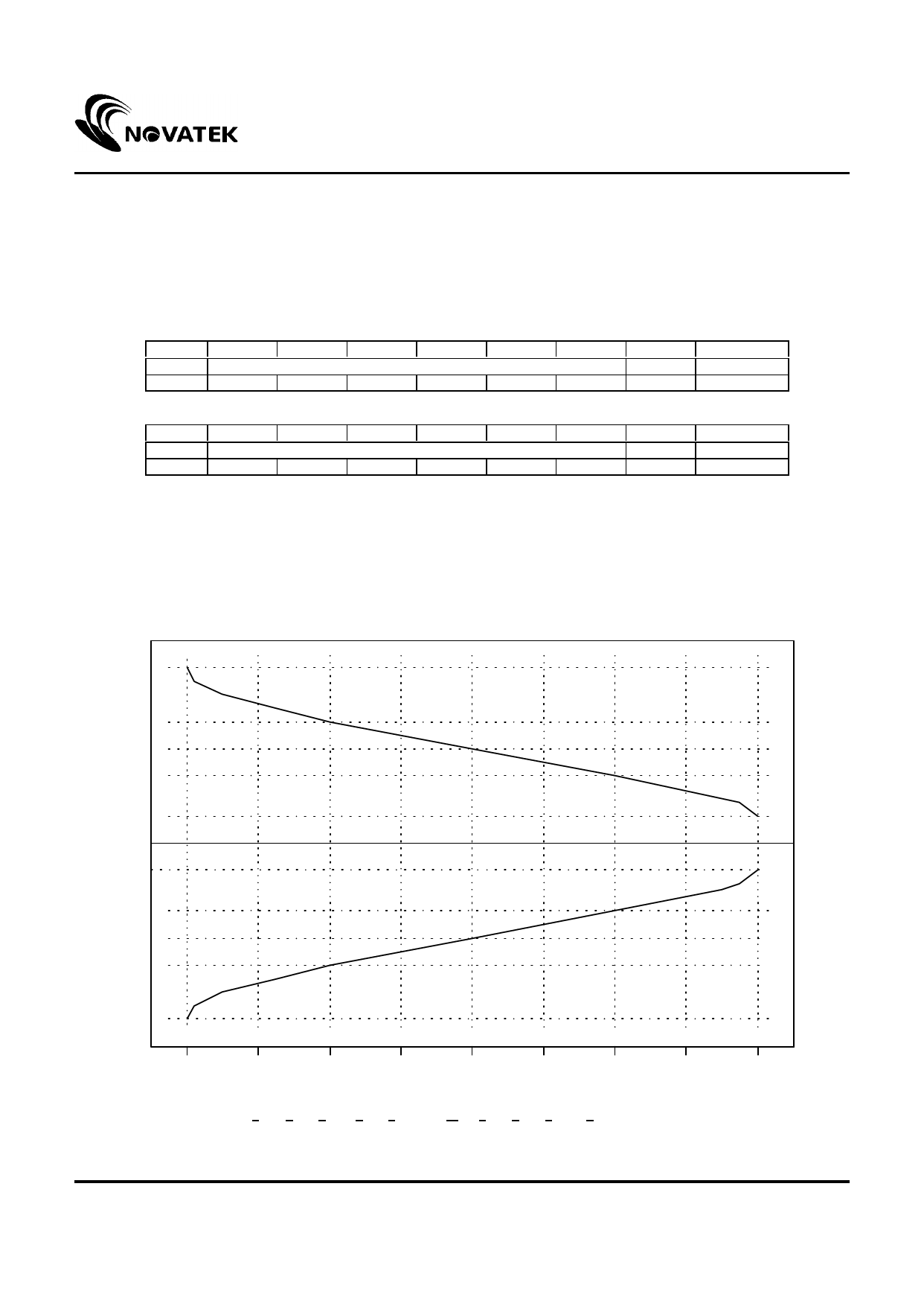
Relationship between input data and output voltage
The figure below shows the relationship between the input data and the output voltage with the polarity. The range of V1~V5
is for positive polarity, and V6 ~ V10 for negative polarity. Please refer to the following page to get the relative resister value
and voltage calculation method.
Gamma correction diagram
Vout
AVDD
V1
V2
V3
V4
V5
Vcom
V6
V7
V8
V9
Positive polarity
Negative polarity
V10
AVSS
00H
08H
10H
18H
20H
28H
30H
38H
3FH Input Data
Remark: AVDD-0.1 > V1 > V2 > V3 > V4 > V5; V6 > V7 > V8 > V9 > V10 >AVSS+0.1V
4
Version 2.0
Share Link: 