NT3965 Ver la hoja de datos (PDF) - Novatek Microelectronics
Número de pieza
componentes Descripción
Fabricante
NT3965 Datasheet PDF : 12 Pages
| |||
NT3965
TFT LCD Source Driver
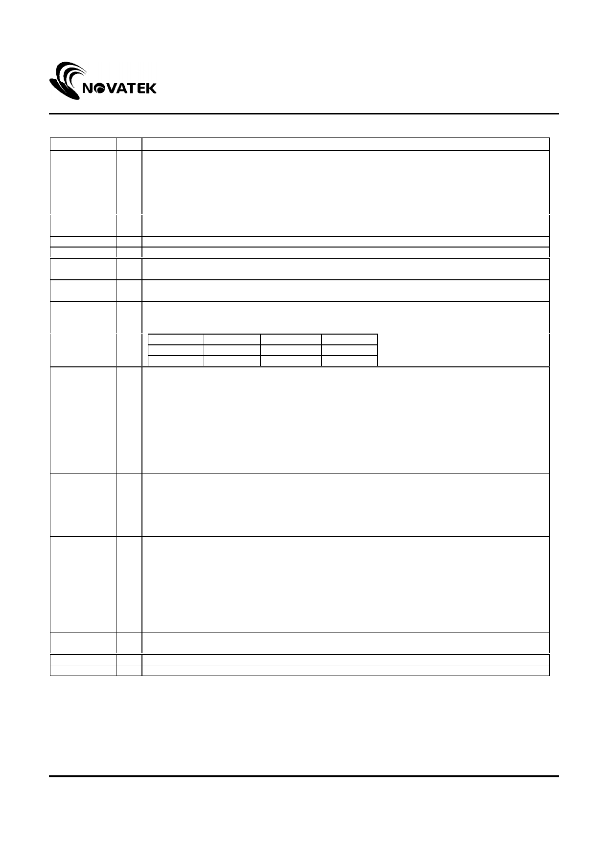
Pin Description
Designation
D05 ~ D00
D15 ~ D10
D25 ~ D20
D35 ~ D30
D45 ~ D40
D55 ~ D50
REV1
REV2
CLK
V1 ~ V10
OUT1 ~
OUT384
SHL
DIO1
DIO2
LD
POL
AVDD
AVSS
Vcc
GND
I/O
Description
I
Data input. For six 6-bit, 2 pixels, of color data (R, G, B)
DX5 : MSB; DX0 : LSB
I
Controls whether the D00~D25 data are inverted or not.
When “REV1”=1 these data will be inverted. EX. “00” à “ 3F”, “07”à “ 38”, “15”à “2A,” and so on.
I Controls whether the data of D30~D55 are inverted or not, same as REV1.
I Clock input; latching data onto the line latches at the rising edge.
I
Gamma correction reference voltage. The voltage of these pins must be AVSS< V10< V9<
V8<V7<V6; V5<V4<V3<V2<V1< AVDD
O Output drive signals
Selects left or right shift;
SHL=“1” : DIO1àOUT1,2,3,4,5,6àOUT7,8,9,10,11,12--àOUT379,380,381,382,383,384= DIO2
I
SHL=“0” : DIO1=OUT1,2,3,4,5,6ßOUT7,8,9,10,11,12ß-- OUT379,380,381,382,383,384ßDIO2
SHL
DIO1
DIO2
SHIFT
1
Input
Output
Right
0
Output
Input
Left
Start pulse signal input/output
When SHL is applied high (SHL="1"), a start high-pulse on DIO1 is latched at the rising edge of the
CLK. Then the data are latched serially onto internal latches at the rising edge of the CLK. After all
line latches are filled with data, 64 clocks, a pulse is shifted out through the DIO2 pin at the rising
I/O
edge of the CLK. This function can cascade two or more devices for dot-size expansion. In normal
applications, the DIO2 signal of the first device is connected to the DIO1 of the second stage, and
the DIO2 of the second one is connected to the DIO1 of the third, and so on, in a chain.
In contrast, when SHL is applied low, a start pulse inputs on DIO2, and a pulse outputs through
DIO1.
*Remark: The input pulse-width of DIO1/2 may be over 1 clock-cycle.
Latches the polarity of outputs and switches the new data to outputs.
1. At the rising edge, latches the “POL” signal to control the polarity of the outputs.
I 2. This pin also controls the switch of the line registers that switches the new incoming data to
outputs .
*Remark: The LD may switch the new data to outputs at anytime even if the line data are not
completely full.
Polarity selector for the dot-inversion control. Available at the rising edge of LD
“POL” value is latched at the rising edge of “LD” to control the polarity of the even or odd outputs.
“POL=1” represents that even outputs are of positive polarity with a voltage range from V1~V5, and
odd outputs are of negative polarity with a voltage range from V6 to V10. On the other hand, if LD
I gets low level “POL”, even outputs are of negative polarity and odd outputs are of positive polarity.
POL=1: Even outputs range from V1 ~ V5
Odd outputs range from V6 ~ V10
POL=0: Even outputs range from V6 ~ V10
Odd outputs range from V1 ~ V5
I Power supply for analog circuit
I Ground pin for analog circuit
I Power supply for digital circuit
I Ground pin for digital circuit
3
Version 2.0
Share Link: 