DS2180A Ver la hoja de datos (PDF) - Dallas Semiconductor -> Maxim Integrated
Número de pieza
componentes Descripción
Fabricante
DS2180A Datasheet PDF : 35 Pages
| |||
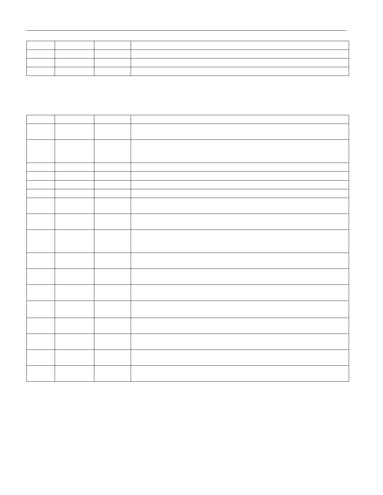
POWER AND TEST PIN DESCRIPTION (40-PIN DIP ONLY) Table 3
PIN SYMBOL TYPE
DESCRIPTION
20
VSS
32
TEST
40
VDD
-
Signal Ground. 0.0 volts.
I
Test Mode. Tie to VSS for normal operation.
-
Positive Supply. 5.0 volts.
DS2180A
RECEIVE PIN DESCRIPTION (40-PIN DIP ONLY) Table 4
PIN SYMBOL TYPE
DESCRIPTION
21
RYEL
0
Receive Yellow Alarm. Transitions high when yellow alarm detected, goes low
when alarm clears.
22
RLINK
0
Receive Link Data. Updated with extracted FDL data one RCLK before start of
odd frames (193E) and held until next update. Updated with extracted S-bit data one
RCLK before start of even frames (193S) and held until next update.
23
RLCLK
0
Receive Link Clock. 4 kHz demand clock for RLINK.
24
RCLK
I
Receive Clock. 1.544 MHz primary clock.
25
RCHCLK
O
Receive Channel Clock. 192 kHz clock identifies time slot (channel) boundaries.
26
RSER
O
Receive Serial Data. Received NRZ serial data, updated on rising edges of RCLK.
27
RFSYNC
O
Receive Frame Sync. Extracted 8 kHz clock, one RCLK wide, indicates F-Bit
position in each frame.
28
RMSYNC
O
Receive Multiframe Sync. Extracted multiframe sync; edge indicates start of
multiframe, 50% duty cycle.
29
RABCD
O
Receive ABCD Signaling. Extracted signaling data output, valid for each channel
time in signaling frames. In non-signaling frames, RABCD outputs the LSB of each
channel word.
30
RSIGFR
O
Receive Signaling Frame. High during signaling frames, low during resync and
non-signaling frames.
31
RSIGSEL
O
Receive Signaling Select. In 193E framing a .667 kHz clock which identifies
signaling frames A and C. A 1.33 kHz clock in 193S.
33
RST
I
Reset. A high-low transition clears all internal registers and resets receive side
counters. A high-low-high transition will initiate a receive resync.
34
RPOS
35
RNEG
I
Receive Bipolar Data Inputs. Samples on falling edge of RCLK. Tie together to
receive NRZ data and disable bipolar violation monitoring circuitry.
36
RCL
O
Receive Carrier Loss. High if 32 consecutive 0's appear at RPOS and RNEG; goes
low after next 1.
37
RBV
O
Receive Bipolar Violation. High during accused bit time at RSER if bipolar
violation detected, low otherwise.
38
RFER
O
Receive Frame Error. High during F-Bit time when FT or FS errors occur (193S)
or when FPS or CRC errors occur (193E). Low during resync.
39
RLOS
O
Receive Loss of Sync. Indicates sync status; high when internal resync is in
progress, low otherwise.
4 of 35
Share Link: 