ADE7759 Ver la hoja de datos (PDF) - Analog Devices
Número de pieza
componentes Descripción
Fabricante
ADE7759 Datasheet PDF : 36 Pages
| |||
Test Circuits
VDD
I
10F
100nF
100nF
10F
1k⍀
33nF
RB
1k⍀
33nF
110V
1k⍀ 33nF
600k⍀
1k⍀ 33nF
10F 100nF
CT TURN RATIO = 1800:1
CHANNEL 2 GAIN = 1
GAIN (CH1) RB
1
10⍀
4
2.5⍀
AVDD DVDD RESET
DIN
V1P
DOUT
SCLK
V1N U1
ADE7759 CS
CLKOUT
V2N
CLKIN
V2P
REFIN/OUT
IRQ
SAG
ZX
CF
AGND DGND
TO SPI BUS
(USED ONLY FOR
CALIBRATION)
Y1
3.58MHz
22pF
22pF
NOT CONNECTED
U3
TO
FREQUENCY
COUNTER
PS2501-1
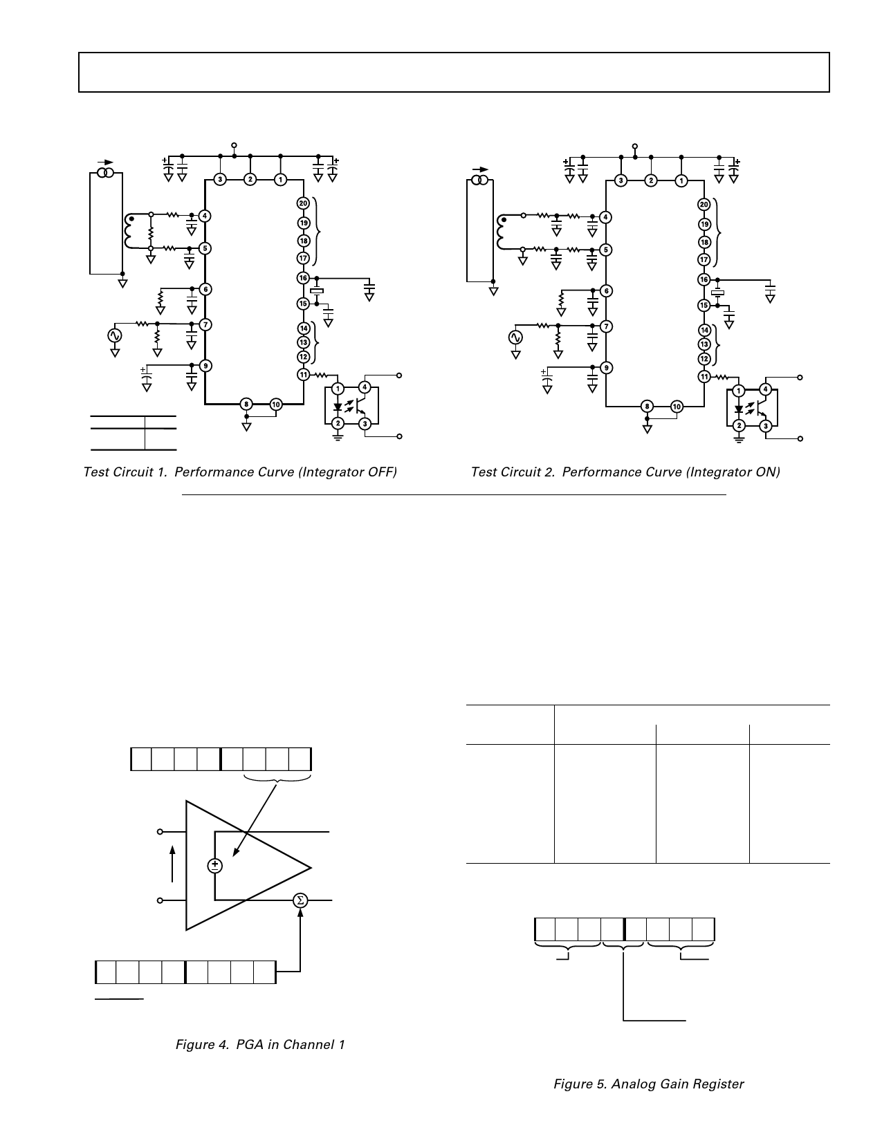
Test Circuit 1. Performance Curve (Integrator OFF)
ADE7759
VDD
I
10F
100nF
100nF
10F
di/dt CURRENT
SENSOR
100⍀ 1k⍀
33nF 33nF
100⍀ 1k⍀
33nF 33nF
110V
1k⍀ 33nF
600k⍀
1k⍀ 33nF
10F 100nF
CHANNEL 1 GAIN = 4
CHANNEL 2 GAIN = 1
AVDD
V1P
DVDD
RESET
DIN
DOUT
SCLK
V1N U1
ADE7759 CS
CLKOUT
V2N
CLKIN
V2P
REFIN/OUT
IRQ
SAG
ZX
CF
AGND DGND
TO SPI BUS
(USED ONLY FOR
CALIBRATION)
Y1
3.58MHz
22pF
22pF
NOT CONNECTED
U3
TO
FREQUENCY
COUNTER
PS2501-1
Test Circuit 2. Performance Curve (Integrator ON)
ANALOG INPUTS
The ADE7759 has two fully differential voltage input channels.
The maximum differential input voltage for input pairs V1P/V1N
and V2P/V2N are ± 0.5 V. In addition, the maximum signal
level on analog inputs for V1P/V1N and V2P/V2N are ± 0.5 V
with respect to AGND.
Each analog input channel has a PGA (Programmable Gain
Amplifier) with possible gain selections of 1, 2, 4, 8, and 16. The
gain selections are made by writing to the gain register—see
Figure 5. Bits 0 to 2 select the gain for the PGA in Channel 1 and
the gain selection for the PGA in Channel 2 is made via Bits 5
to 7. Figure 4 shows how a gain selection for Channel 1
is made using the gain register.
GAIN[7:0]
GAIN (K)
SELECTION
V1P
VIN
K ؋ VIN
V1N
+
OFFSET ADJUST
(؎50mV)
CH1OS[7:0]
BIT 0 to 5: SIGN MAGNITUDE CODED OFFSET CORRECTION
BIT 6: NOT USED
BIT 7: DIGITAL INTEGRATOR (ON = 1, OFF = 0; DEFAULT ON)
Figure 4. PGA in Channel 1
In addition to the PGA, Channel 1 also has a full-scale input
range selection for the ADC. The ADC analog input range
selection is also made using the gain register—see Figure 5. As
mentioned previously the maximum differential input voltage is
0.5 V. However, by using Bits 3 and 4 in the gain register, the
maximum ADC input voltage can be set to 0.5 V, 0.25 V, or
0.125 V. This is achieved by adjusting the ADC reference—see
Reference Circuit section. Table I summarizes the maximum
differential input signal level on Channel 1 for the various ADC
range and gain selections.
Table I. Maximum Input Signal Levels for Channel 1
Max Signal
Channel 1
ADC Input Range Selection
0.5 V
0.25 V
0.125 V
0.5 V
0.25 V
0.125 V
0.0625 V
0.0313 V
0.0156 V
0.00781 V
Gain = 1
Gain = 2
Gain = 4
Gain = 8
Gain = 16
Gain = 1
Gain = 2
Gain = 4
Gain = 8
Gain = 16
Gain = 1
Gain = 2
Gain = 4
Gain = 8
Gain = 16
GAIN REGISTER*
CHANNEL 1 AND CHANNEL 2 PGA CONTROL
76 54 32 10
00
00
00
0 0 ADDR:
0AH
PGA 2 GAIN SELECT
000 = ؋1
001 = ؋2
010 = ؋4
011 = ؋8
100 = ؋16
*REGISTER CONTENTS
SHOW POWER-ON DEFAULTS
PGA 1 GAIN SELECT
000 = ؋1
001 = ؋2
010 = ؋4
011 = ؋8
100 = ؋16
CHANNEL 1 FULL-SCALE SELECT
00 = 0.5V
01 = 0.25V
10 = 0.125V
REV. A
–11–
Figure 5. Analog Gain Register
Share Link: 