CXK5B81020J-12 Ver la hoja de datos (PDF) - Sony Semiconductor
NГәmero de pieza
componentes DescripciГіn
Fabricante
CXK5B81020J-12 Datasheet PDF : 9 Pages
| |||
CXK5B81020J/TM
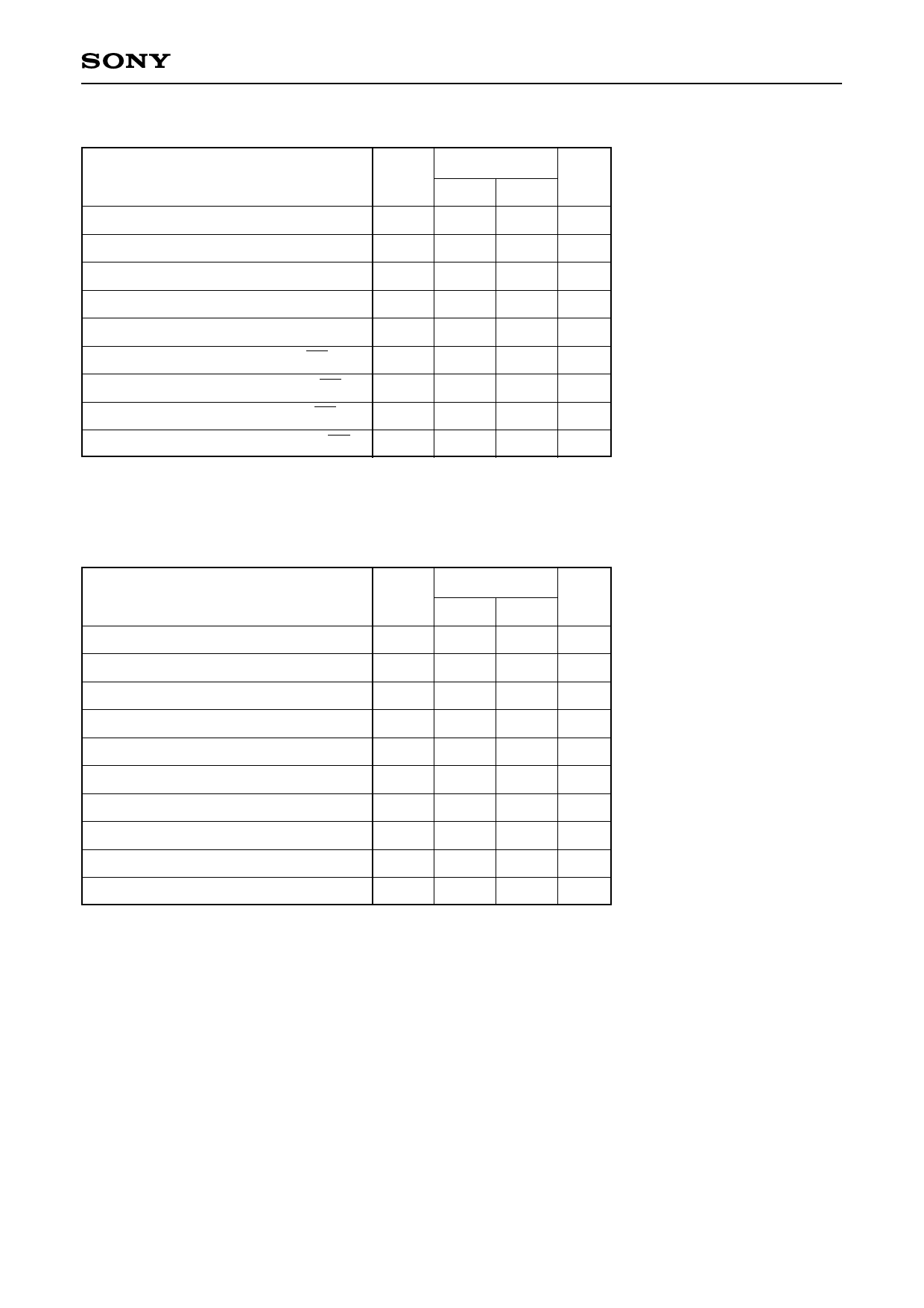
вҖў Read cycle
-12
Item
Symbol
Unit
Min. Max.
Read cycle time
tRC
12
вҖ”
ns
Address access time
tAA
вҖ”
12
ns
Chip enable access time
tCO
вҖ”
12
ns
Output enable to output valid
tOE
вҖ”
6
ns
Output data hold time
tOH
3
вҖ”
ns
Chip enable to output in low Z (CE)
tLZ
3
вҖ”
ns
Output enable to output in low Z (OE) tOLZвҲ—
0
вҖ”
ns
Chip disable to output in high Z (CE)
tHZвҲ—
0
6
ns
Output disable to output in high Z (OE) tOHZвҲ—
0
6
ns
вҲ— Transition is measured Вұ200mV from steady voltage with specified loading in Fig. 1 1-(2).
This parameter is sampled and is not 100% tested.
вҖў Write cycle
-12
Item
Symbol
Unit
Min. Max.
Write cycle time
tWC
12
вҖ”
ns
Address valid to end of write
tAW
10
вҖ”
ns
Chip enable to end of write
tCW
10
вҖ”
ns
Data valid to end of write
tDW
8
вҖ”
ns
Data hold from end of write
tDH
0
вҖ”
ns
Write pulse width
tWP
10
вҖ”
ns
Address set up time
tAS
0
вҖ”
ns
Write recovery time
tWR
0
вҖ”
ns
Output active from lend of write
tOWвҲ—
4
вҖ”
ns
Write to output in high Z
tWHZвҲ—
0
6
ns
вҲ— Transition is measured Вұ200mV from steady voltage with specified loading in Fig. 1 1-(2).
This parameter is sampled and is not 100% tested.
вҖ“4вҖ“
Share Link: 