SC1102A Ver la hoja de datos (PDF) - Semtech Corporation
Número de pieza
componentes Descripción
Fabricante
SC1102A
Semtech Corporation

SC1102A Datasheet PDF : 12 Pages
| |||
POWER MANAGEMENT
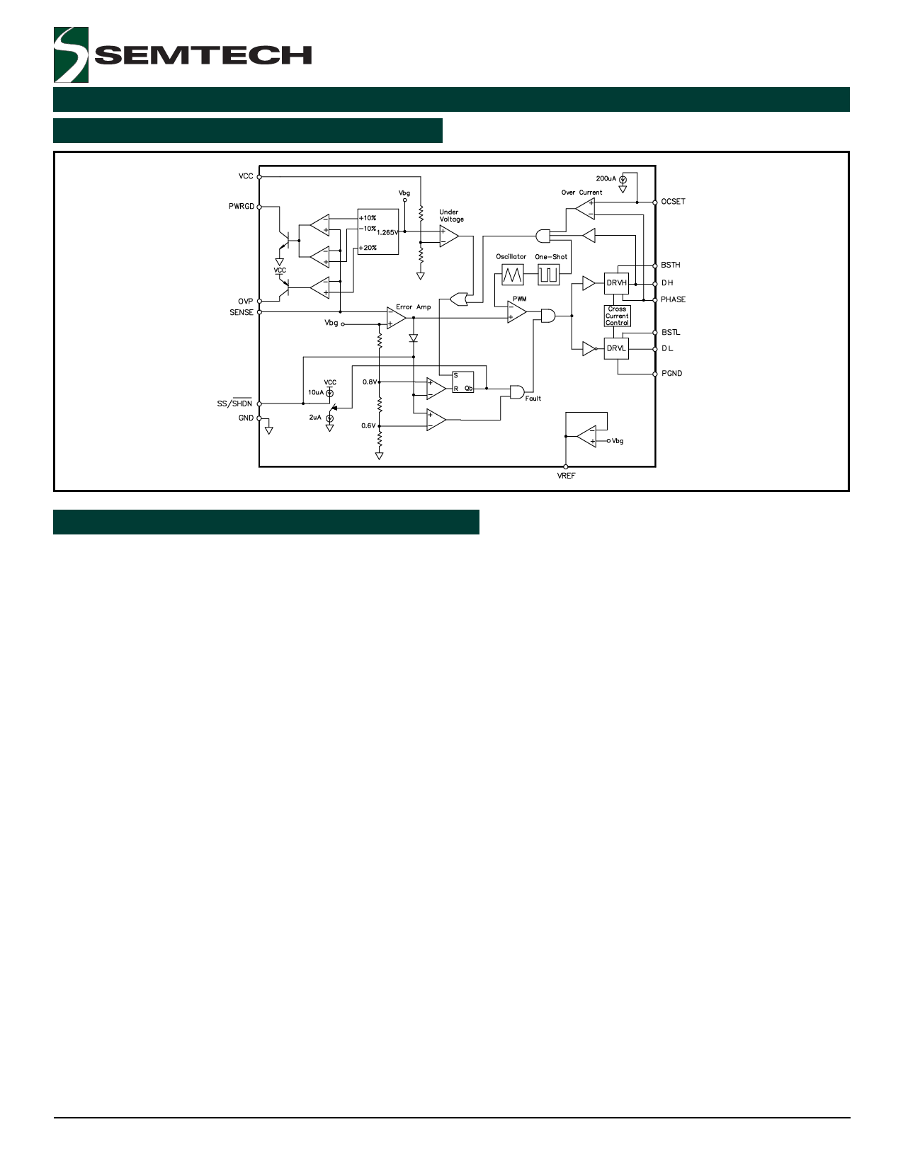
Block Diagram
SC1102/SC1102A
Applications Information - Theory of Operation
Synchronous Buck Converter
Primary VCORE power is provided by a synchronous, volt-
age-mode pulse width modulated (PWM) controller. This
section has all the features required to build a high effi-
ciency synchronous buck converter, including “Power
Good” flag, shut-down, and cycle-by-cycle current limit.
The output voltage of the synchronous converter is set
and controlled by the output of the error amplifier. The
external resistive divider reference voltage is derived from
an internal trimmed-bandgap voltage reference (See Fig.
1). The inverting input of the error amplifier receives its
voltage from the SENSE pin.
The internal oscillator uses an on-chip capacitor and
trimmed precision current sources to set the oscillation
frequency to 200kHz/500kHz. The triangular output of
the oscillator sets the reference voltage at the inverting
input of the comparator. The non-inverting input of the
comparator receives it’s input voltage from the error am-
plifier. When the oscillator output voltage drops below
the error amplifier output voltage, the comparator out-
put goes high. This pulls DL low, turning off the low-side
FET, and DH is pulled high, turning on the high-side FET
(once the cross-current control allows it). When the oscil-
lator voltage rises back above the error amplifier output
voltage, the comparator output goes low. This pulls DH
low, turning off the high-side FET, and DL is pulled high,
turning on the low-side FET (once the cross-current con-
trol allows it).
As SENSE increases, the output voltage of the error
amplifier decreases. This causes a reduction in the on-
time of the high-side MOSFET connected to DH, hence
lowering the output voltage.
Under Voltage Lockout
The under voltage lockout circuit of the SC1102 assures
that the high-side MOSFET driver outputs remain in the
off state whenever the supply voltage drops below set
parameters. Lockout occurs if VCC falls below 4.1V. Nor-
mal operation resumes once VCC rises above 4.2V.
Over-Voltage Protection
The over-voltage protection pin (OVP) is high only when
the voltage at SENSE is 20% higher than the target value
programmed by the external resistor divider. The OVP pin
is internally connected to a PNP’s collector.
Power Good
The power good function is to confirm that the regulator
outputs are within +/-10% of the programmed level.
PWRGD remains high as long as this condition is met.
PWRGD is connected to an internal open collector NPN
transistor.
2006 Semtech Corp.
5
www.semtech.com
Share Link: