LTC1515 Ver la hoja de datos (PDF) - Linear Technology
Número de pieza
componentes Descripción
Fabricante
LTC1515 Datasheet PDF : 8 Pages
| |||
LTC1515 Series
APPLICATIONS INFORMATION
Output Voltage Selection
The LTC1515-X versions have internal resistor networks
which set the output voltage. The 5/3 pin controls an
internal switch that shorts out a portion of the resistor
network to change the output voltage. A logic high on this
pin produces a 5V output and a low produces either a 3V
output or a 3.3V output.
The output voltage of the LTC1515 is selected using an
external resistor divider (see Figure 1). The output voltage
is determined using the following formula:
VOUT = (1.232V)[1 + (R1/R2)]
The total resistance of R1 and R2 should not exceed 2M,
otherwise excess ripple may appear at VOUT.
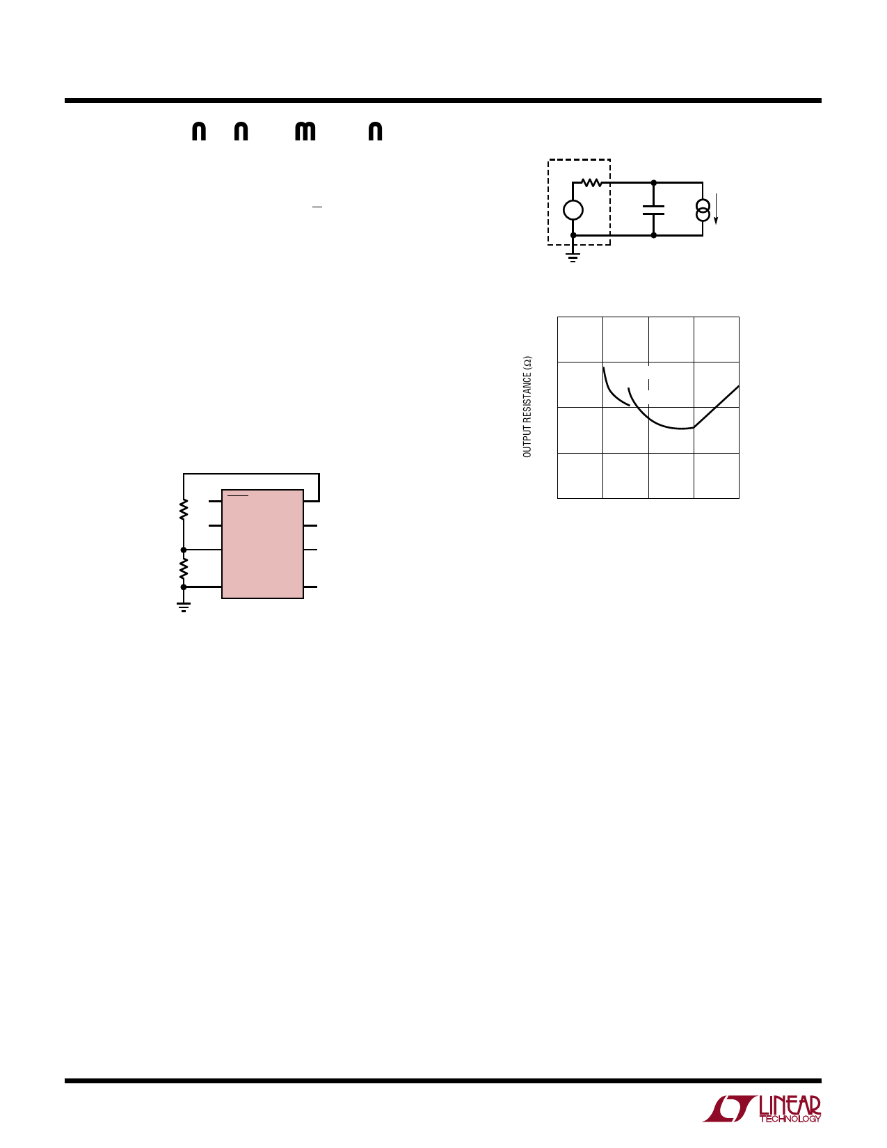
ROUT
+– 2VIN
+
VOUT
–
COUT
IOUT
LT1515 • F02
Figure 2. Step-Up Mode Equivalent Circuit
40
30
IOUT = 20mA
IOUT = 50mA
20
10
1 SHDN
R1
2 POR
VOUT 8
7
VIN
3
FB
LTC1515
C1+
6
R2
4
GND
C1– 5
LTC1515 • F01
Figure 1. LTC1515 Output Voltage Selection
Maximum VOUT and IOUT Calculations for the LTC1515
The maximum output voltage and current available with
the LTC1515 can be calculated based on the effective
output resistance of the charge pump and the open circuit
output voltage. In step-up mode, the open circuit output
voltage is approximately 2VIN (see Figure 2). In step-down
mode, the open circuit output voltage equals VIN. The
relationship between ROUT and VIN in step-up mode is shown
in Figure 3.
The following formulas can be used to find the maximum
output voltage that may be programmed using the LTC1515
for a given minimum input voltage and output current
load.
Step-Up Mode: Max VOUT = (2)(Min VIN) – (IOUT)(ROUT)
Step-Down Mode: Max VOUT = (Min VIN) – (IOUT)(ROUT)
When VIN – (IOUT)(ROUT) is less than the programmed
VOUT, the part will automatically switch from step-down
mode to step-up mode. In both step-up mode and step-
0
1
2
3
4
5
INPUT VOLTAGE (V)
LT1515 • F03
Figure 3. Step-Up Mode ROUT vs Input Voltage
down mode, ROUT is internally adjusted to ensure that the
maximum output current rating can be met.
Capacitor Selection
For best performance, low ESR capacitors are recom-
mended for both CIN and COUT to reduce noise and ripple.
The CIN and COUT capacitors should be either ceramic or
tantalum and should be 10µF or greater. If the input source
impedance is very low (< 0.5Ω) CIN may not be needed.
Increasing the size of COUT to 22µF or greater will reduce
output voltage ripple — particularly with high VIN voltages
(8V or greater). A ceramic capacitor is recommended for
the flying capacitor C1 with a value of 0.1µF or 0.22µF.
Smaller values may be used in low output current
applications.
Output Ripple
Normal LTC1515 series operation produces voltage ripple
on the VOUT pin. Output voltage ripple is required for the
parts to regulate. Low frequency ripple exists due to the
hysteresis in the sense comparator and propagation de-
lays in the charge pump enable/disable circuits. High
frequency ripple is also present mainly from the ESR
6
Share Link: 