STA002 Ver la hoja de datos (PDF) - STMicroelectronics
Número de pieza
componentes Descripción
Fabricante
STA002 Datasheet PDF : 43 Pages
| |||
STA002
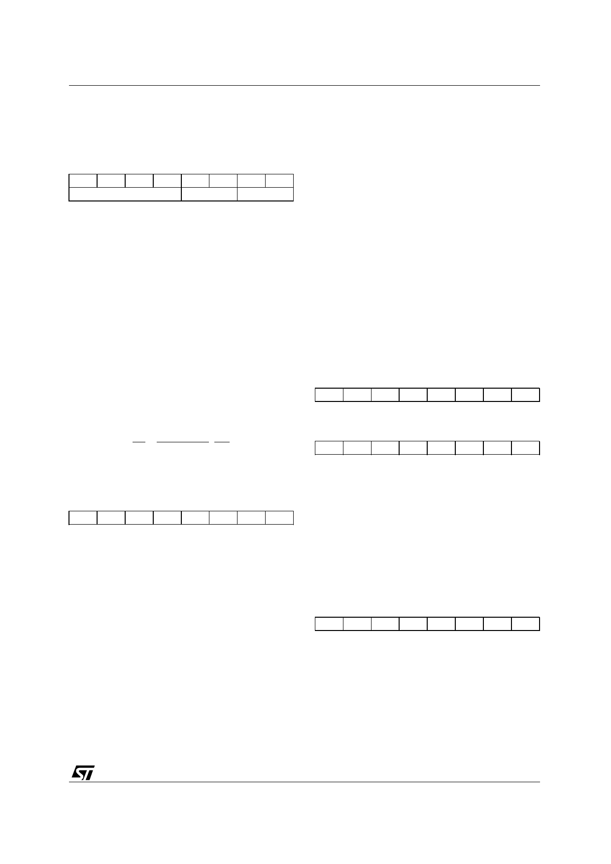
QPSK_CONTROL2 Register
Internal address: 81 H
Reset Value: 90H
MSB
b7 b6 b5 b4 b3 b2
PFDTHR
CNTHR
LSB
b1 b0
SN
The threshold value depends on the signal level
at the Nyquist filter output. A good value for this
parameter is given by: PFDTHR = 0.4 AGC2REF
where AGC2REF is the reference value for the
AGC2 loop.
3.4.4 Internal ramp parameter
In presence of a frequency offset greater than the
pull-in range of the carrier loop or in presence of
low signal to noise ratio the tracking performance
of the loop itself may became rather slow. To
help the loop in tracking this frequency offset an
internal ramp can be activated by I2C bus.
This ramp can be switched on or off by setting
the SWON parameter 1 or 0 respectively. When
SWON=0 the output value of the ramp is null.
The sweep rate can be calculated by the follow-
ing formula:
dF
dt
=
2swstep
stepper +
1
Fc2k
226
where swstep can only take 0 and 1 values and
stepper can be programmed in a range from 0 to 15.
MSB
LSB
X X b5 b4 b3 b2 b1 b0
b5 : SWON; 1 = 2 ramp on; 0 = 2 ramp off
b4 : SWSTEP
b3 - b0 : STEPPER
Ramp control register (RAMPCTRL)
Internal address: 95 H
Reset Value: 01H
3.5. AGC1
3.5.1 AGC1 control
To avoid a degradation of the signal to noise ratio
a constant IF level is necessary at the channel
decoder input.
The AGC1 outputs a signal to control the Variable
Gain Amplifier in the RF Front-End in order to
mantain a fixed level at the ADC input.
The input signal power (computed after the A/D
conversion) is compared to a programmable
threshold; the difference is scaled by the
AGC1BETA coefficient then integrated.
The result is converted into a pulse width modula-
tion signal to drive the AGC output pin; it may be
filtered by a simple RC filter to control the gain
command of a variable gain amplifier before the
A to D conversion.
The 8 integrator MSB’s (AGC1_ INTG register)
may be read or written at any time by the micro;
when written, the LSB’s are reset.
The integrator value is the level of the AGC out-
put, after low pass filtering; it gives an image of
the input signal power. The sign of the loop can
be controlled by the AGC1CHS control bit in the
QPSK_CONTROL1 register in order to adapt the
loop to a positive or negative slope of the variable
gain amplifier.
3.5.2 Registers
AGC1 reference level register (AGC1_REF)
Internal address: 83 H 82H
Reset Value : 01H 06H
MSB
LSB
X X X X X X b9 b8
AGC1_REF2
MSB
LSB
b7 b6 b5 b4 b3 b2 b1 b0
AGC1_REF1
This register is divided into two bytes. The LSB
byte is named AGC1_REF1, the MSB is named
AGC1_REF2.
The reset value of this register (262) maintains
the peak signal input level equal to the half range
of the ADC.
AGC1 integrator gain register (AGC1_BETA)
Internal address: 84 H
Reset Value: 00H
MSB
LSB
X X X X X b2 b1 b0
AGC1_BETA
The AGC1 loop gain βAGC1 is given by:
bAGC1 = 2AGC1_BETA
The parameter AGC1_BETA can only take values
from 0 to 5. When AGC1_BETA is set to "111"
the loop gain is null. This condition is useful to
open the AGC1 loop.
19/43
Share Link: 