ST3917B Ver la hoja de datos (PDF) - STMicroelectronics
Número de pieza
componentes Descripción
Fabricante
ST3917B Datasheet PDF : 16 Pages
| |||
ST3917A - ST3917B
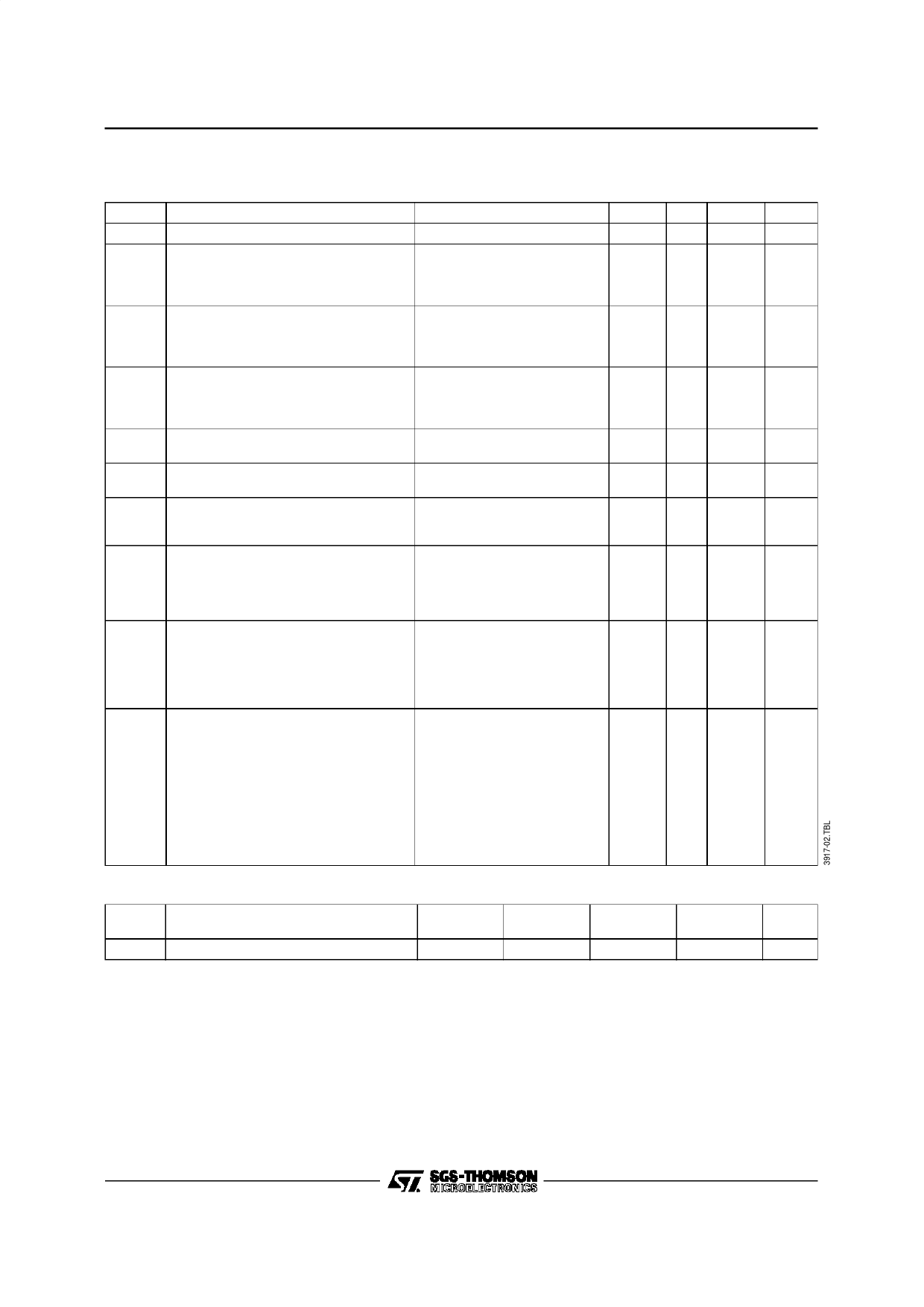
ELECTRICAL CHARACTERISTICS (continued)
(ILN = 10mA to 120mA, f = 1kHz, Tamb = 25°C, VDD = 3V ; unless otherwise specified)
Symbol
Parameter
Test Conditions
Min. Typ.
ZDTMF
GRX
AGRX
DRX
NRX
ZOUT
DTMF Attenuation Pin Impedance
Receive gain (see Figure 11)
Receive Gain Variation (see Figure 11)
Receive Distortion (see Figure 11)
Receive Noise (see Figure 11)
Receive Output Impedance
(see Figure 11)
VINP = 4mVRMS,
RE = 300Ω, RGRX=100kΩ
ILN = 15mA
ILN = 60mA
VINP = 4mVRMS,
RE = 300Ω, ILN = 15MA
RGRX = 10KΩ
RGRX = 300kΩ
ILN = 15mA, RGRX=100kΩ
RE = 150Ω, VEAR = 0.25VRMS
RE = 300Ω, VEAR = 0.45VRMS
RE = 450Ω, VEAR = 0.55VRMS
ILN = 15mA, RE = 300Ω
RGRX = 100kΩ, VINP = 0V
ILN = 15mA
25
29.5
23.0
-20
32
31.0
25.0
-20
+10
200
35
VPT Pacifier Tone Level on Earphone
ILN = 15mA
(see Figure 11)
RP = ∞
60
RP = 430kΩ
600
Keyboard Interface
See Figures 4 and 5
TKD Keypad Debounce Time
32
FKS Keypad Scan Frequency
250
KRU Keypad Pullup Resistance
100
KRD Keypad Pulldown Resistance
500
TRIS
TR
TPSD
TISD
TDUR
Tone Mode
Tone Output Rise Time
Tone Signalling Rate
Presignal Delay
Intersignal Delay
Tone Output Duration
See Figures 2 and 3
5.55
40
90
90
Pulse Mode
See Figures 4 and 5
TPT Pacifier Tone Duration
75
FPT Pacifier Tone Frequency
500
PR
Pulse Rate
10
TB
Break Time :
ST3917A
60
ST3917B
67
TM
Make Time :
ST3917A
40
ST3917B
33
IDP Interdigital Pause
820
PDP Predigital Pause : ST3917A
50
ST3917B
43
Max.
39
32.5
27.0
10
2
2
2
5
Unit
kΩ
dB
dB
dB
dB
dB
%
%
%
µV
Ω
mVRMS
mVRMS
ms
Hz
kΩ
Ω
ms
1/sec
ms
ms
ms
ms
Hz
PPS
ms
ms
ms
ms
ms
ms
ms
Option Selectable
Symbol
Parameter
Option 1 Option 2 Option 3 Option 4
SEL = VDD SEL = GND SEL = ROW SEL = COL
Unit
tFLASH Timed Hook Flash (see Figures 2 and3)
100
600
300
100
ms
Notes : 1. All inputs unloaded. Quiescent mode (oscillator off).
2. Pulse output sink current for VOUT = 0.5V at VDD = 3V.
3. Pacifier tone sink current for VOUT = 0.5V, source current for VOUT = 2.5V at VDD = 3V.
4. Memory retention voltage is the point where memory is guaranteed but circuit operation is not. Proper memory retention is
guaranteed if either the minimum IMR is provided or the minimum VMR. The design does not have to provide both the minimum
current and voltage.
5. Option 1 is with softswitch inhibition.
7/16
Share Link: 