TEA6321 Ver la hoja de datos (PDF) - Philips Electronics
Número de pieza
componentes Descripción
Fabricante
TEA6321 Datasheet PDF : 36 Pages
| |||
Philips Semiconductors
Sound fader control circuit
Preliminary specification
TEA6321
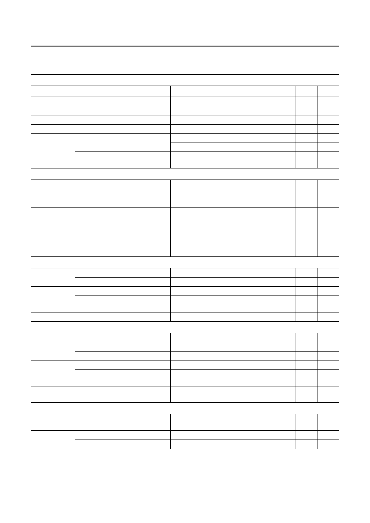
SYMBOL
PARAMETER
CONDITIONS
∆Ga
∆Gt
MUTEatt
Voffset
attenuator set error
gain tracking error
mute attenuation
DC step offset between any
adjoining step
DC step offset between any step to
mute
Gv = +20 to −50 dB
Gv = −51 to −66 dB
Gv = +20 to −50 dB
see Fig.10
Gv = 0 to −66 dB
Gv = 20 to 0 dB
Gv = 0 to −66 dB
Volume I control and loudness
CRvol
Gv
Gstep
LBmax
continuous volume control range
voltage gain
step resolution
maximum loudness boost
loudness on; referred to
loudness off; boost is
determined by external
components
f = 40 Hz
f = 10 kHz
Bass control
Gbass
bass control, maximum boost
maximum attenuation
f = 46 Hz
f = 46 Hz
Gstep
step resolution (toggle switching)
step error between any adjoining
step
f = 46 Hz
f = 46 Hz
Voffset
DC step offset in any bass position
Treble control
Gtreble
Gstep
Voffset
treble control, maximum boost
maximum attenuation
maximum boost
step resolution (toggle switching)
step error between any adjoining
step
DC step offset in any treble
position
f = 15 kHz
f = 15 kHz
f > 15 kHz
f = 15 kHz
f = 15 kHz
Volume II, balance and fader control
CR
Gstep
continuous attenuation fader and
volume control range
step resolution
attenuation set error
MIN.
−
−
−
100
−
−
−
TYP.
−
−
−
110
0.2
2
−
MAX. UNIT
2
dB
3
dB
2
dB
−
dB
10
mV
15
mV
10
mV
−
51
−31 −
−
1
−
dB
+20 dB
−
dB
−
17
−
dB
−
4.5 −
dB
16
18
19
dB
16
18
19
dB
−
1.8 −
dB
−
−
0.5 dB
−
−
20
mV
11
12
13
dB
11
12
13
dB
−
−
15
dB
−
1.5 −
dB
−
−
0.5 dB
−
−
10
mV
53.5 55
−
1
−
−
56.5 dB
2
dB
1.5 dB
1995 Dec 19
9
Share Link: 