LG1628BXA Ver la hoja de datos (PDF) - Agere -> LSI Corporation
Número de pieza
componentes Descripción
Fabricante
LG1628BXA Datasheet PDF : 12 Pages
| |||
Preliminary Data Sheet
January 1998
LG1628AXA SONET/SDH 2.488 Gbits/s
Transimpedance Amplifier
Die Pad Configuration (continued)
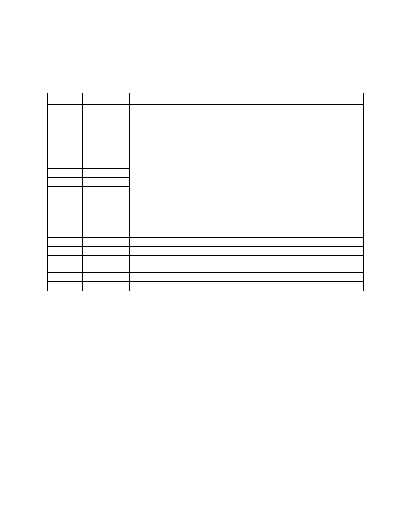
The pad descriptions for the LG1628AXA are given in Table 1.
Table 1. Pad Descriptions
Pad
1
2, 19, 23
3
4
5
6
7
8
9
10
Symbol
IN+
GND1
BYPASS
OP2OUT
OP1OUT
OP1–
OP1+
OP2–
OP2+A
OP2+B
Description
Amplifier input; connect to detector anode, current should enter this node.
Ground.
Connections between these nodes and an external dual op amp form the over-
load control circuitry. See the test circuit in Figure 4 for wiring details.
To operate the amplifier without overload control connect OP2OUT to VSS,
OP1OUT to GND, and leave BYPASS and the remaining op amp connections
open (Figure 5).
11
12
13, 16, 18
14
15
17
20, 21, 22
24
VSS1
VSS2
GND2
OUT–
OUT+
BG
DNC
IN–
Supply voltage; –5.2 Vdc nominal.
Supply voltage; –5.2 Vdc nominal.
Ground.
Inverted data output (produces low-level output for current entering IN+).
Noninverted data output (produces high-level output for current entering IN+).
Connection for external –2.5 Vdc voltage reference (typically use an Si band-
gap).
Do not connect; internal test point or reserved for future use.
Inverting input; must provide ac bypass to ground when using overload control.
Lucent Technologies Inc.
3
Share Link: 