BTS650PE3180A Ver la hoja de datos (PDF) - Infineon Technologies
Número de pieza
componentes Descripción
Fabricante
BTS650PE3180A Datasheet PDF : 16 Pages
| |||
Data Sheet BTS650P
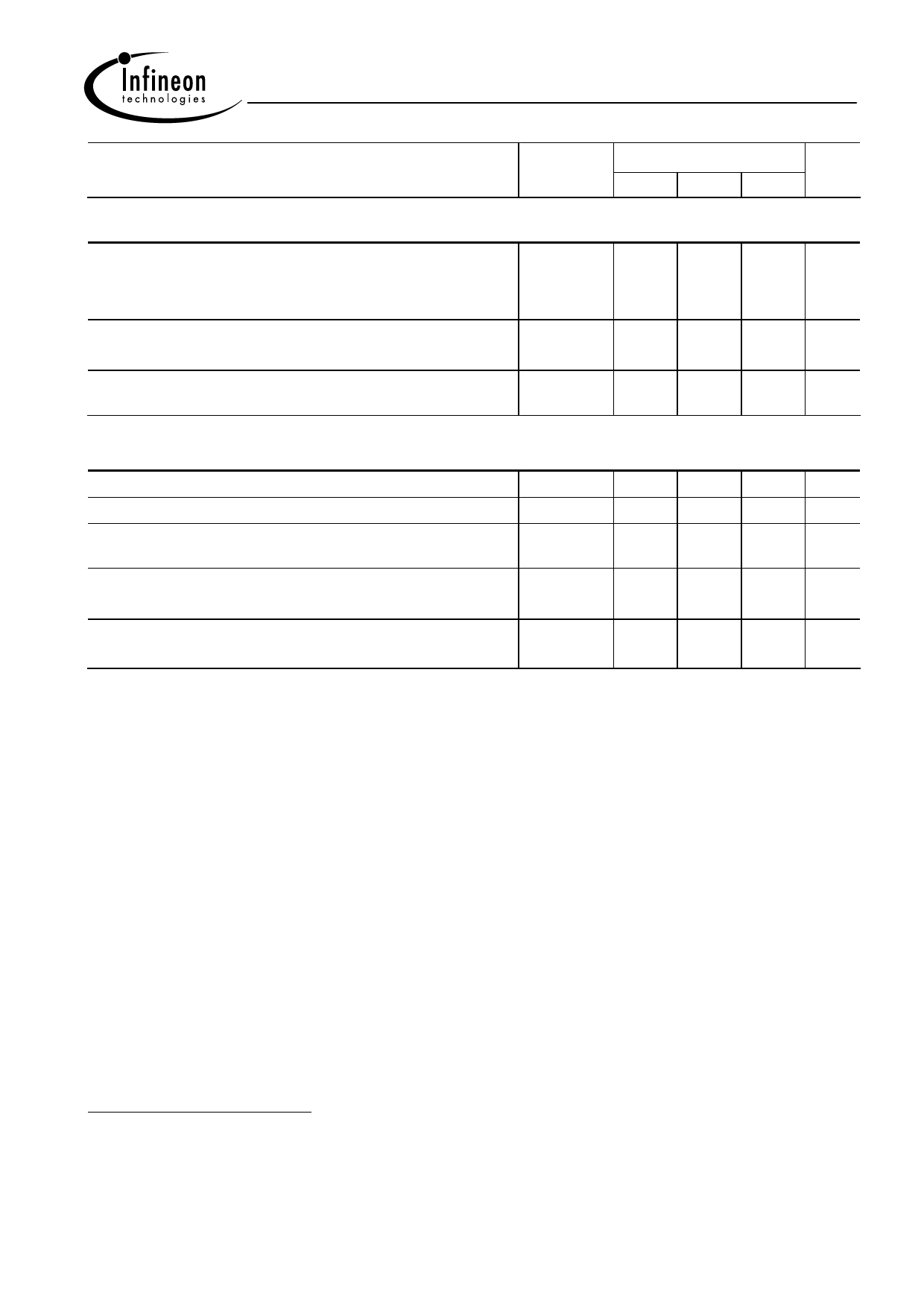
Parameter and Conditions
at Tj = -40 ... +150 °C, Vbb = 12 V unless otherwise specified
Symbol
Inverse Load Current Operation
On-state resistance (Pins 1, 2, 6, 7 to pin 4)
VbIN = 12 V, IL = - 20 A
Tj = 25 °C:
see diagram on page 10
Tj = 150 °C:
Nominal inverse load current (Pins 1, 2, 6, 7 to Tab)
VON = -0.5 V, Tc = 85 °C11
Drain-source diode voltage (Vout > Vbb)
IL = - 20 A, IIN = 0, Tj = +150°C
RON(inv)
IL(inv)
-VON
Operating Parameters
Operating voltage (VIN = 0V) 13)
Under voltage shutdown 14)
Under voltage start of charge pump
see diagram page 15
Over voltage protection 15)
Ibb = 15 mA
Tj =-40°C:
Tj = 25...+150°C:
Standby current
IIN = 0
Tj =-40...+25°C:
Tj = 150°C:
Vbb(on)
VbIN(u)
VbIN(ucp)
VZ,IN
Ibb(off)
Values
Unit
min typ max
-- 4.4 6.0 mΩ
7.9 10.5
55 70
-- A
-- 0.6
-- V
5.0
-- 34 V
1.5 3.0 4.5 V
3.0 4.5 6.0 V
60
--
-- V
62 66
--
-- 15 25 µA
-- 25 50
13) If the device is turned on before a Vbb-decrease, the operating voltage range is extended down to VbIN(u).
For all voltages 0 ... 34 V the device is fully protected against overtemperature and short circuit.
14) VbIN = Vbb - VIN see diagram on page 7. When VbIN increases from less than VbIN(u) up to VbIN(ucp) = 5 V
(typ.) the charge pump is not active and VOUT ≈Vbb - 3 V.
15) See also VON(CL) in circuit diagram on page 9.
Infineon Technologies AG
Page 4
2003-Oct-01
Share Link: 