TE28F400B3T110 Ver la hoja de datos (PDF) - Intel
Número de pieza
componentes Descripción
Fabricante
TE28F400B3T110 Datasheet PDF : 48 Pages
| |||
E
SMART 3 ADVANCED BOOT BLOCK
1.0 INTRODUCTION
This datasheet contains the specifications for the
Advanced Boot Block flash memory family, which is
optimized for low power, portable systems. This
family of products features 1.65 V–2.5 V or 2.7 V–
3.6 V I/Os and a low VCC/VPP operating range of
2.7 V–3.6 V for read, program, and erase
operations. In addition this family is capable of fast
programming at 12 V. Throughout this document,
the term “2.7 V” refers to the full voltage range
2.7 V–3.6 V (except where noted otherwise) and
“VPP = 12 V” refers to 12 V ±5%. Section 1.0 and
2.0 provide an overview of the flash memory family
including applications, pinouts and pin descriptions.
Section 3.0 describes the memory organization and
operation for these products. Sections 4.0 and 5.0
contain the operating specifications. Finally,
Sections 6.0 and 7.0 provide ordering and other
reference information.
1.1 Smart 3 Advanced Boot Block
Flash Memory Enhancements
The Smart 3 Advanced Boot Block flash memory
features
• Enhanced blocking for easy segmentation of
code and data or additional design flexibility
• Program Suspend to Read command
• VCCQ input of 1.65 V–2.5 V on all I/Os. See
Figures 1 through 4 for pinout diagrams and
VCCQ location
• Maximum program and erase time specification
for improved data storage.
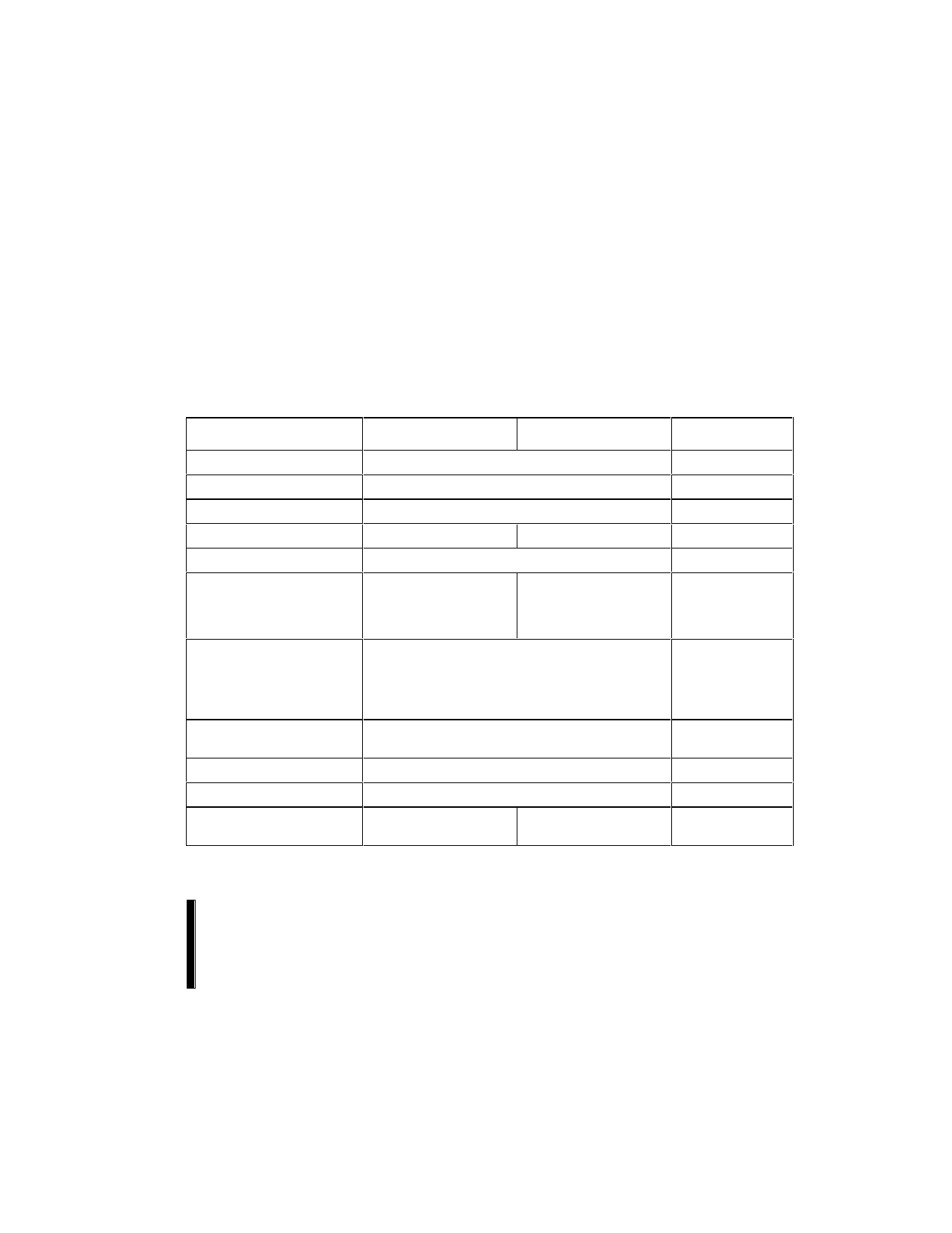
Feature
Table 1. Smart 3 Advanced Boot Block Feature Summary
28F008B3, 28F016B3, 28F400B3(2), 28F800B3,
28F032B3(1)
28F160B3, 28F320B3
Reference
VCC Read Voltage
2.7 V– 3.6 V
Section 4.2, 4.4
VCCQ I/O Voltage
1.65 V–2.5 V or 2.7 V– 3.6 V
Section 4.2, 4.4
VPP Program/Erase Voltage
2.7 V– 3.6 V or 11.4 V– 12.6 V
Section 4.2, 4.4
Bus Width
8-bit
16 bit
Table 3
Speed
80 ns, 90 ns, 100 ns, 110 ns
Section 4.5
Memory Arrangement
1024 Kbit x 8 (8 Mbit),
2048 Kbit x 8 (16 Mbit),
4096 Kbit x 8 (32 Mbit)
256 Kbit x 16 (4 Mbit),
512 Kbit x 16 (8 Mbit),
1024 Kbit x 16 (16 Mbit)
2048 Kbit x 16 (32 Mbit)
Section 2.2
Blocking (top or bottom)
Eight 8-Kbyte parameter blocks and
Seven 64-Kbyte blocks (4-Mbit) or
Fifteen 64-Kbyte blocks (8-Mbit) or
Thirty-one 64-Kbyte main blocks (16-Mbit)
Sixty-three 64-Kbyte main blocks (32-Mbit)
Section 2.2
Appendix D
Locking
WP# locks/unlocks parameter blocks
All other blocks protected using VPP
Section 3.3
Table 8
Operating Temperature
Extended: –40 °C to +85 °C
Section 4.2, 4.4
Program/Erase Cycling
100,000 cycles
Section 4.2, 4.4
Packages
40-lead TSOP(1), 48-Ball 48-Lead TSOP, 48-Ball Figure 3, Figure 4
µBGA* CSP(2)
µBGA CSP(2)
NOTES:
1. 4-Mbit and 32-Mbit density not available in 40-lead TSOP.
2. 4-Mbit density not available in µBGA* CSP.
PRELIMINARY
5
Share Link: 