L6246 Ver la hoja de datos (PDF) - STMicroelectronics
Número de pieza
componentes Descripción
Fabricante
L6246 Datasheet PDF : 12 Pages
| |||
L6246
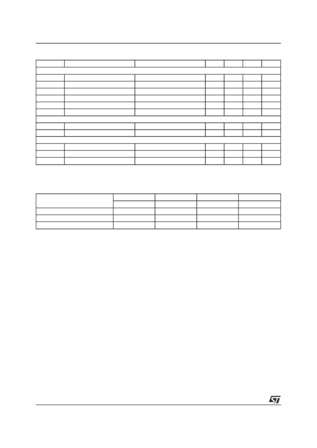
ELECTRICAL CHARACTERISTICS (continued)
Symbol
Parameter
POWER AMPLIFIER
Rdson DMOS on resistance
Gdv
Differential voltage gain
Iol
Output current leakage
SR
Output slew rate
Tsr
Saturation recovery time
GBW Gain bandwidth product
RETRACT
Vr
Max. retract voltage
Vr
Max. retract voltage
CHARGE PUMP
Cs
Storage capacitor
Vs
Storage voltage
Cp
Pump capacitor
Test Condition
at 25°C
Vcc shorted to GND
Vcc Normal
Min. Typ. Max. Unit
0.3
Ω
32
V/V
500
µA
0.4
V/µs
5
µs
100
KHz
300 mV
1
V
Vcc +4
1
µF
V
0.2
µF
RETRACT TRUTH TABLE
Brake and Retract
Run
Disable
Inp ut
-Retract
0
1
1
Inp ut
+Enable
X
1
0
Out put
Bridge Enable
0
1
0
Out put
+Retract
1
0
0
BLOCK DESCRIPTION
POWER AMPLIFIERS
The two power amplifiers are connected in bridge
configuration working in AB class.
SENSE AMPLIFIER
This stage senses the voltage drop across the
Rsense.
The input stage is supplied by the charge pump
voltage to have an high dynamic, while the other
sections of the amplifier are supplied by the volt-
age of 10.5V internally regulated to have an high
power supply rejection (this voltage, supplies also
the error amplifier, the input amplifier and the op-
erational amplifier which generates the Vcc/2 volt-
age).
The open loop gain is around 80dB and the band-
with is more than 1MHz.
The voltage gain is fixed internally at 10 V/V.
ERROR AMPLIFIER
This is the stage which compares the input volt-
age and the sense voltage, generating the control
voltage for the power section.
The open loop gain and bandwith of this amplifier
are similar to the sense amplifier.
The negative input and the output of the error am-
plifier are accessible externally in order to have
the current loop compensation user configurable.
The dynamic of the output is limited at +/- 2Vbe to
have a faster response of the output voltage.
INPUT AMPLIFIER
The inputs and the output pins are externally ac-
cessible to have the possibility to configure the
transconductance gain of the current control loop
selecting the voltage gain of this amplifier.
The open loop gain and bandwith of this amplifier
are similar to the sense amplifier.
REFERENCE VOLTAGE GENERATOR
This block generates the two reference voltage
Vcc/2 and +5VREF.
The Vcc/2 voltage is used as reference by the
current control loop.
The +5VREF is a very stable voltage generator
that can be used as reference voltage of an exter-
nal DAC.
6/12
Share Link: 